
 German
 Japanese
 Portuguese
 Korea
Korea
 Mexico
 Dutch
Dutch


Why Choose Us?
Professional Platform
B2B & B2C purchasingDelivery at full speed
1-2 days deliveryWide variety
Original manufacturers365 days guarantee
Responsible quality
.png)


Tech Specifications
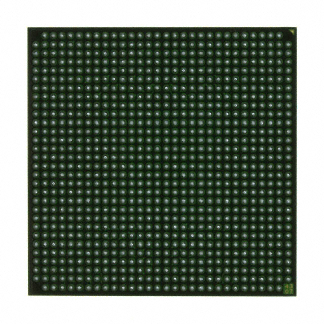
XC2V1000-5FF896I Description
The XC2V1000-5FF896I is a field programmable gate array (FPGA) device manufactured by Advanced Micro Devices (AMD). This device is designed to provide high-performance and flexible solutions for a wide range of applications.
Description:
The XC2V1000-5FF896I is a member of the Virtex-II Pro family of FPGAs. It is a high-performance device with a large number of programmable logic elements, making it suitable for complex and demanding applications. The device is available in a 5FF896I package, which is a flip-chip ball grid array (FCBGA) package with a total of 896 I/O (input/output) pins.
Features:
Some of the key features of the XC2V1000-5FF896I include:
- High-performance programmable logic: The device offers a large number of programmable logic elements, including configurable logic blocks (CLBs), digital signal processing blocks (DSPs), and block RAM (BRAM).
- High-speed transceivers: The device includes high-speed transceivers that support data rates up to 6.6 Gbps, making it suitable for high-speed communication applications.
- Advanced I/O capabilities: The device supports a wide range of I/O standards, including LVDS, PCI Express, and Gigabit Ethernet, making it suitable for a wide range of applications.
- Integrated hard intellectual property (IP): The device includes a range of pre-built IP cores, such as memory controllers, processors, and interface protocols, which can help reduce development time and effort.
- Low power consumption: The device is designed to operate at low power levels, making it suitable for applications where power consumption is a critical factor.
Applications:
The XC2V1000-5FF896I is suitable for a wide range of applications, including:
- High-speed communication systems: The device's high-speed transceivers and advanced I/O capabilities make it suitable for applications such as telecommunications, networking, and data center infrastructure.
- Signal processing: The device's digital signal processing blocks and programmable logic elements make it suitable for applications such as image and video processing, radar and sonar systems, and medical imaging.
- Embedded systems: The device's integrated hard IP and low power consumption make it suitable for applications such as industrial control systems, automotive systems, and consumer electronics.
- Aerospace and defense: The device's high performance and reliability make it suitable for applications in aerospace and defense, such as satellite systems, radar systems, and secure communications.
Overall, the XC2V1000-5FF896I is a powerful and versatile FPGA device that offers a range of features and capabilities suitable for a wide range of applications.
FAQ
Not available to buy online? Want the lower wholesale price? Please Send RFQ to get best price, we will respond immediately


.png?x-oss-process=image/format,webp/resize,h_32)


