
AMD
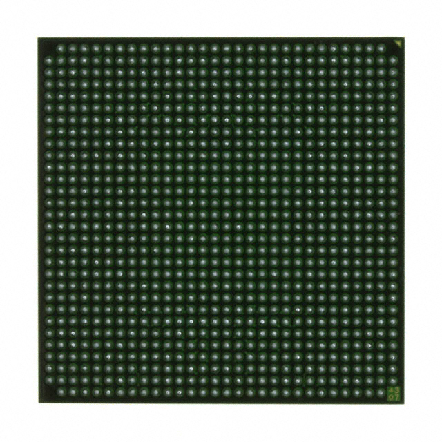
XC2VP20-5FFG896C
FPGAs


.png?x-oss-process=image/format,webp/resize,p_30)


XC2VP20-5FFG896C Description
The XC2VP20-5FFG896C is a field programmable gate array (FPGA) from AMD (Advanced Micro Devices). This device is designed for use in a variety of applications, including embedded systems, digital signal processing, and communications systems.
Description:
The XC2VP20-5FFG896C is a mid-range FPGA that offers a balance of performance, power efficiency, and cost-effectiveness. It is based on AMD's Virtex-II Pro series of FPGAs, which are known for their high performance and advanced features.
Features:
Some of the key features of the XC2VP20-5FFG896C include:
- High-performance logic cells: The device contains a large number of configurable logic cells, which can be used to implement a wide range of digital logic functions.
- Dedicated digital signal processing (DSP) blocks: The FPGA includes dedicated DSP blocks that can be used for high-speed mathematical operations, such as multiplication and accumulation.
- High-speed I/O: The device supports a wide range of high-speed I/O interfaces, including LVDS, GTP, and PCI Express.
- Internal memory: The FPGA includes a large amount of internal memory, which can be used for data storage and processing.
- Configurable logic blocks: The device includes configurable logic blocks that can be used to implement a wide range of digital logic functions.
- Low power consumption: The XC2VP20-5FFG896C is designed to operate with low power consumption, making it suitable for use in battery-powered or energy-sensitive applications.
Applications:
The XC2VP20-5FFG896C is suitable for a wide range of applications, including:
- Embedded systems: The device can be used in embedded systems that require high performance and low power consumption, such as industrial control systems and automotive infotainment systems.
- Digital signal processing: The FPGA's dedicated DSP blocks make it well-suited for applications that require high-speed mathematical operations, such as audio and video processing.
- Communications systems: The high-speed I/O interfaces and configurable logic blocks make the XC2VP20-5FFG896C suitable for use in communications systems, such as base stations and routers.
- Military and aerospace: The device's performance, reliability, and radiation tolerance make it suitable for use in military and aerospace applications, such as satellite communications and radar systems.
- Test and measurement: The FPGA's versatility and configurability make it well-suited for use in test and measurement equipment, such as oscilloscopes and spectrum analyzers.
Overall, the XC2VP20-5FFG896C is a versatile and powerful FPGA that offers a range of features and capabilities that make it suitable for a wide range of applications.
Tech Specifications
XC2VP20-5FFG896C Documents
Download datasheets and manufacturer documentation for XC2VP20-5FFG896C
 Virtex-II Pro, Pro X
  Mult Dev EOL 6/Jan/2020
  Virtex-II Pro, Pro X
  Xilinx REACH211 Cert Xiliinx RoHS Cert
 Relevant Search
Shopping Guide


.png?x-oss-process=image/format,webp/resize,h_32)


