
 German
 Japanese
 Portuguese
 Korea
Korea
 Mexico
 Dutch
Dutch


Why Choose Us?
Professional Platform
B2B & B2C purchasingDelivery at full speed
1-2 days deliveryWide variety
Original manufacturers365 days guarantee
Responsible quality
.png)


Tech Specifications
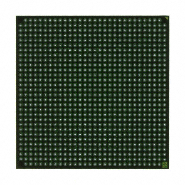
XC2VP30-6FFG896I Description
The XC2VP30-6FFG896I is a field programmable gate array (FPGA) device manufactured by Advanced Micro Devices (AMD). This device is designed for use in a wide range of applications that require high-performance, low-power, and flexible programmability.
Description:
The XC2VP30-6FFG896I is a member of the Virtex-II Pro family of FPGAs from AMD. It is a high-performance, low-power device that offers a range of features and capabilities for a variety of applications. The device is available in a fine-pitch ball grid array (FBGA) package with a total of 896 I/O (input/output) pins.
Features:
Some of the key features of the XC2VP30-6FFG896I include:
- High-performance logic cells: The device features a large number of high-performance logic cells that can be configured to perform a wide range of functions.
- Dedicated digital signal processing (DSP) blocks: The device includes dedicated DSP blocks that can be used for high-speed mathematical operations and other signal processing tasks.
- High-speed transceivers: The device includes high-speed transceivers that can be used for data transmission and reception in a variety of communication protocols.
- On-chip memory: The device includes a range of on-chip memory resources, including block RAM and distributed RAM, that can be used for data storage and processing.
- Integrated hard intellectual property (IP): The device includes a range of pre-built hard IP blocks that can be used to implement common functions such as clock management, input/output interfaces, and memory controllers.
Applications:
The XC2VP30-6FFG896I is a versatile FPGA device that can be used in a wide range of applications, including:
- Communications: The device can be used in a variety of communication systems, including wireless base stations, routers, and switches.
- Military and aerospace: The device is designed to meet the stringent reliability and performance requirements of military and aerospace applications.
- Industrial control: The device can be used in a variety of industrial control systems, including motor control, power management, and process control.
- Medical electronics: The device can be used in a range of medical electronics applications, including imaging systems, patient monitoring, and diagnostic equipment.
- Automotive: The device can be used in a variety of automotive applications, including infotainment systems, advanced driver assistance systems (ADAS), and powertrain control.
In summary, the XC2VP30-6FFG896I is a high-performance, low-power FPGA device from AMD that offers a range of features and capabilities for a variety of applications. Its versatility, combined with its high performance and low power consumption, make it an excellent choice for a wide range of applications in communications, military and aerospace, industrial control, medical electronics, and automotive.
FAQ
Not available to buy online? Want the lower wholesale price? Please Send RFQ to get best price, we will respond immediately


.png?x-oss-process=image/format,webp/resize,h_32)


