
 German
 Japanese
 Portuguese
 Korea
Korea
 Mexico
 Dutch
Dutch


Why Choose Us?
Professional Platform
B2B & B2C purchasingDelivery at full speed
1-2 days deliveryWide variety
Original manufacturers365 days guarantee
Responsible quality
.png)


Tech Specifications
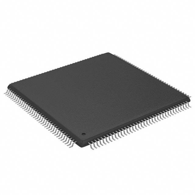
XC6SLX9-2TQG144C Description
The XC6SLX9-2TQG144C is a field programmable gate array (FPGA) device manufactured by AMD (Advanced Micro Devices). Here is a description of the model, its features, and potential applications:
Model Description:
The XC6SLX9-2TQG144C is a member of the Spartan-6 series of FPGAs. It is a mid-range device designed for a wide range of applications that require a balance between performance, power consumption, and cost.
Features:
- Logic Capacity: The XC6SLX9-2TQG144C offers a high-density of programmable logic resources, suitable for complex digital designs.
- I/O Count: It comes with a large number of input/output (I/O) pins, which can be configured for various types of interfaces.
- Speed Grade: The "-2" in the model number indicates a speed grade that operates at a maximum frequency of 228 MHz.
- Package Type: The "TQG144C" denotes a thin quad flat package (TQFP) with 144 pins, which is a common package type for mid-range FPGAs.
- Power Consumption: Spartan-6 FPGAs are designed with power efficiency in mind, making them suitable for battery-powered or energy-sensitive applications.
- Integrated Memory: The device includes block RAM (BRAM) and other memory resources that can be used for data storage and processing tasks.
- DSP Blocks: It may include digital signal processing (DSP) blocks for high-speed arithmetic operations.
- Serdes Capabilities: The FPGA may support high-speed serial transceivers for interfacing with external devices or networks.
- Configurability: The device can be programmed to implement a wide range of digital logic functions, making it highly versatile.
Applications:
The XC6SLX9-2TQG144C is suitable for a variety of applications due to its balance of performance and cost:
- Communication Systems: It can be used in the design of communication interfaces, including Ethernet, serial communication, and wireless interfaces.
- Industrial Control: For implementing complex control algorithms in industrial automation and robotics.
- Video Processing: It can handle video processing tasks, such as image and signal processing, in surveillance systems or professional video equipment.
- Medical Equipment: In medical devices where real-time processing and low power consumption are critical.
- Consumer Electronics: For the development of consumer products that require customizable logic, such as set-top boxes or gaming consoles.
- Military and Aerospace: Due to their robustness and configurability, FPGAs like the XC6SLX9 are used in military and aerospace applications where reliability is paramount.
- Networking Equipment: For designing network routers, switches, and other networking equipment that require flexible and high-speed data processing.
It's important to note that the specific features and capabilities of the XC6SLX9-2TQG144C can vary, and a detailed datasheet should be consulted for precise specifications and to understand the device's full potential in a given application.
FAQ
| Quantity | Unit Price | Ext. Price |
|---|---|---|
| 1+ | $8.30400 | $8.30 |
| 10+ | $7.20172 | $72.02 |
| 60+ | $6.53143 | $391.89 |
| 120+ | $5.96915 | $716.30 |
Not available to buy online? Want the lower wholesale price? Please Send RFQ to get best price, we will respond immediately


.png?x-oss-process=image/format,webp/resize,h_32)


