
 German
 Japanese
 Portuguese
 Korea
Korea
 Mexico
 Dutch
Dutch




Why Choose Us?
Professional Platform
B2B & B2C purchasingDelivery at full speed
1-2 days deliveryWide variety
Original manufacturers365 days guarantee
Responsible quality

.png)


Tech Specifications
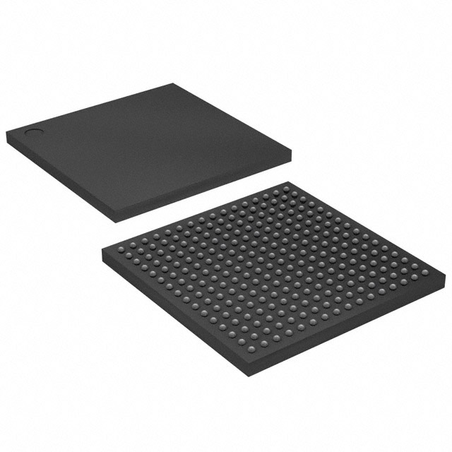
XC6SLX9-3FTG256C Description
The XC6SLX9-3FTG256C is a field programmable gate array (FPGA) device manufactured by Advanced Micro Devices (AMD). This device is part of the Spartan-6 series of FPGAs and is designed to provide high performance and low power consumption for a wide range of applications.
Description:
The XC6SLX9-3FTG256C is a mid-range FPGA that features a high-density of programmable logic resources, making it suitable for a variety of applications. It is available in a flip-chip ball grid array (FCBGA) package with a total of 1,152 I/O (input/output) pins. The device has a programmable logic array of 9,344 slices and a total of 216 digital signal processing (DSP) blocks.
Features:
Some of the key features of the XC6SLX9-3FTG256C include:
- High-density programmable logic resources: The device offers a high-density of programmable logic resources, making it suitable for complex applications that require a large number of gates.
- Low power consumption: The device is designed to operate at low power levels, making it ideal for applications that require low power consumption.
- High-speed transceivers: The device includes high-speed transceivers that support data rates up to 3.125 Gbps, making it suitable for high-speed communication applications.
- Integrated block RAM: The device includes a large amount of block RAM, which can be used to store data and reduce the need for external memory.
- Digital signal processing blocks: The device includes 216 DSP blocks, which can be used to perform complex mathematical operations and signal processing tasks.
Applications:
The XC6SLX9-3FTG256C is suitable for a wide range of applications, including:
- High-speed communication systems: The high-speed transceivers and low power consumption of the device make it ideal for high-speed communication systems, such as 5G base stations and optical transport networks.
- Image and video processing: The device's programmable logic resources and DSP blocks make it well-suited for image and video processing applications, such as video encoding and decoding, image recognition, and machine vision.
- Industrial control systems: The device's I/O capabilities and programmable logic resources make it suitable for industrial control systems, such as motor control and robotics.
- Aerospace and defense: The device's high reliability and radiation tolerance make it suitable for aerospace and defense applications, such as satellite communication systems and radar systems.
- Medical imaging: The device's programmable logic resources and DSP blocks make it well-suited for medical imaging applications, such as computed tomography (CT) and magnetic resonance imaging (MRI) systems.
Overall, the XC6SLX9-3FTG256C is a versatile FPGA device that offers high performance, low power consumption, and a wide range of features that make it suitable for a variety of applications.
FAQ
Not available to buy online? Want the lower wholesale price? Please Send RFQ to get best price, we will respond immediately






.png?x-oss-process=image/format,webp/resize,h_32)


