

Not available to buy online? Want the lower wholesale price? Please Send RFQ to get best price, we will respond immediately


.png?x-oss-process=image/format,webp/resize,p_30)


XC7S25-2CSGA225C Description
XC7S25-2CSGA225C Overview
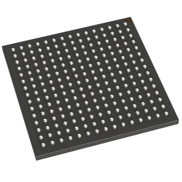
The XC7S25-2CSGA225C integrated circuit belongs to the field programmable gate array (FPGA) family. It is packaged in a tray with a typical package of 1. The device contains 150 input/output (I/O) pins and is surface mountable. There are 1825 logic array blocks/circuit logic blocks (LABs/CLBs) and 23360 logic elements/cells in the XC7S25-2CSGA225C. The device contains 1658880 RAM bits and a voltage supply range of 0.95V to 1.05V. It has an operational temperature range of 0°C to 85°C (TJ) and is packaged in a 225-CSGA (13x13) supplier device package. The XC7S25-2CSGA225C complies with ROHS3 and has an ECCN of EAR99. It is an excellent choice for embedded systems that require a moderate number of I/O pins and RAM.
XC7S25-2CSGA225C Features
Integrated block for PCI Express® (PCIe), for up to x8 Gen3
Endpoint and Root Port designs
Wide variety of configuration options, including support for commodity memories, 256-bit AES encryption with HMAC/SHA-256 authentication, and built-in SEU detection and correction.
High-speed serial connectivity with built-in multi-gigabit transceivers from 600 Mb/s to max rates of 6.6 Gb/s up to 28.05 Gb/s, offering a special low-power mode, optimized for chip-to-chip interfaces.
XC7S25-2CSGA225C Applications
Powerful clock management tiles (CMT), combining phase-locked loop (PLL) and mixed-mode clock manager (MMCM) blocks for high precision and low jitter.
Quickly deploy embedded processing with MicroBlaze™ processor.
Integrated block for PCI Express® (PCIe), for up to x8 Gen3
Tech Specifications
XC7S25-2CSGA225C Documents
Download datasheets and manufacturer documentation for XC7S25-2CSGA225C
 7 Series FPGA Overview Spartan-7 FPGAs Datasheet Xilinx REACH211 Cert Xiliinx RoHS Cert
 Related Parts


Relevant Search
Shopping Guide


.png?x-oss-process=image/format,webp/resize,h_32)


©2025 ERSA Electronics Corporation.