
 German
 Japanese
 Portuguese
 Korea
Korea
 Mexico
 Dutch
Dutch


Why Choose Us?
Professional Platform
B2B & B2C purchasingDelivery at full speed
1-2 days deliveryWide variety
Original manufacturers365 days guarantee
Responsible quality
.png)


Tech Specifications
XC7S25-2FTGB196I Description
XC7S25-2FTGB196I Overview
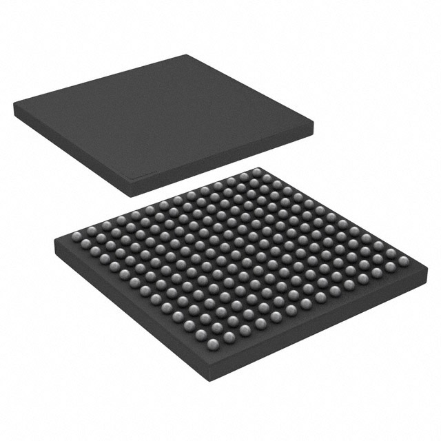
The device features 100 I/Os to promote more efficient data transfer. A basic construction block contains 23360 logic elements or cells. The supply voltage is one volt. Surface Mount connectors link the development board to the FPGA module. To function, the device requires a supply voltage between 0.95 and 1.05 volts. While in usage, operating temperatures should be kept between -40°C and 100°C TJ. To save space, this FPGA model has been contained in Tray. There are a total of 196 terminations. It's worth noting that the device features 1658880 FPGA circuits of RAM. .
XC7S25-2FTGB196I Features
A user configurable analog interface (XADC), incorporating dual 12-bit 1MSPS analog-to-digital converters with on-chip thermal and supply sensors.
Powerful clock management tiles (CMT), combining phase-locked loop (PLL) and mixed-mode clock manager (MMCM) blocks for high precision and low jitter.
Quickly deploy embedded processing with MicroBlaze™ processor.
Integrated block for PCI Express® (PCIe), for up to x8 Gen3
Endpoint and Root Port designs
XC7S25-2FTGB196I Applications
Aerospace & Defense
Telecommunication
Wireless Communications
Voice recognition
Embedded Vision
FAQ
| Quantity | Unit Price | Ext. Price |
|---|---|---|
| 1+ | $37.23280 | $37.23 |
Not available to buy online? Want the lower wholesale price? Please Send RFQ to get best price, we will respond immediately


.png?x-oss-process=image/format,webp/resize,h_32)


