
 German
 Japanese
 Portuguese
 Korea
Korea
 Mexico
 Dutch
Dutch


Why Choose Us?
Professional Platform
B2B & B2C purchasingDelivery at full speed
1-2 days deliveryWide variety
Original manufacturers365 days guarantee
Responsible quality
.png)


Tech Specifications
XC7S25-L1FTGB196I Description
XC7S25-L1FTGB196I Overview
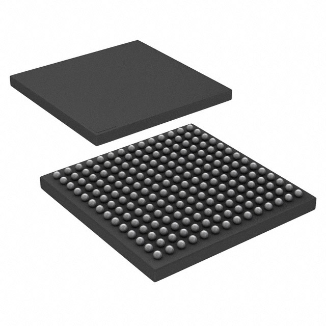
This device is included in the 196-LBGA, CSPBGA package. For speedier data transfer, there are 100 I/Os available. A fundamental construction block is made up of 23360 logic elements/cells. This FPGA module can be used with your development board by connecting it via the Surface Mount connector. It operates on a voltage supply of 0.92V0.98V. The operating temperature of the system should be kept between -40°C and 100°C TJ. To save space, the tray contains a duplicate of this FPGA. This device has 1658880 RAM bits available, which is the entire number of RAM bits. The FPGA is composed of 1825 LABs/CLBs.
XC7S25-L1FTGB196I Features
Endpoint and Root Port designs
Wide variety of configuration options, including support for commodity memories, 256-bit AES encryption with HMAC/SHA-256 authentication, and built-in SEU detection and correction.
Low-cost, wire-bond, bare-die flip-chip, and high signal integrity flip chip packaging offering easy migration between family members in the same package. All packages available in Pb-free and selected packages in Pb option.
Designed for high performance and lowest power with 28 nm, HKMG, HPL process, 1.0V core voltage process technology and 0.9V core voltage option for even lower power.
XC7S25-L1FTGB196I Applications
Consumer Electronics
Aerospace & Defense
Telecommunication
Wireless Communications
Voice recognition
FAQ
Not available to buy online? Want the lower wholesale price? Please Send RFQ to get best price, we will respond immediately


.png?x-oss-process=image/format,webp/resize,h_32)


