
 German
 Japanese
 Portuguese
 Korea
Korea
 Mexico
 Dutch
Dutch


Why Choose Us?
Professional Platform
B2B & B2C purchasingDelivery at full speed
1-2 days deliveryWide variety
Original manufacturers365 days guarantee
Responsible quality
.png)


Tech Specifications
XC7S50-L1CSGA324I Description
XC7S50-L1CSGA324I Overview
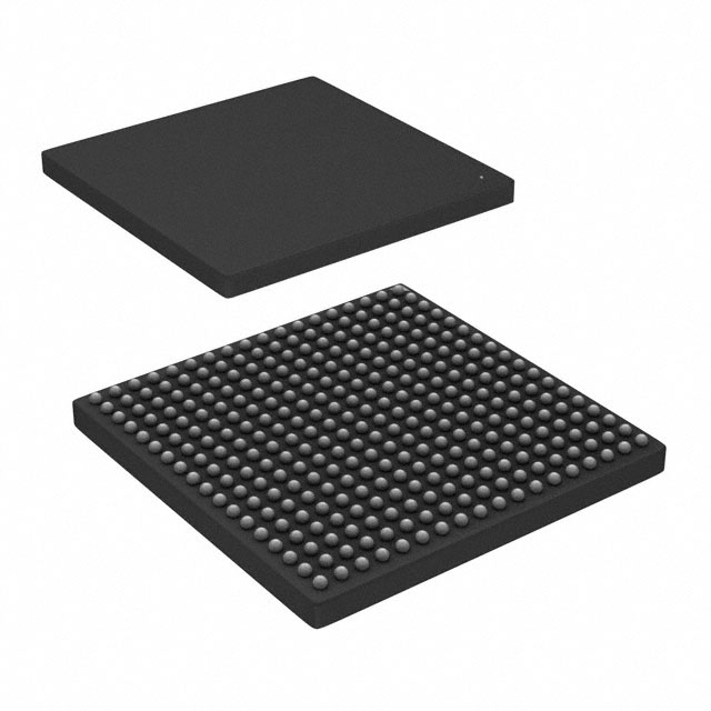
The XC7S50-L1CSGA324I is an FPGA integrated circuit with 4075 LABs/CLBs, 52160 logic elements/cells, and 2764800 total RAM bits. It contains 210 I/Os and a supply voltage range of 0.92V to 0.98V. The device is packaged in a 324-CSPBGA (15x15) supplier device package and operates from -40°C to 100°C (TJ). The XC7S50-L1CSGA324I is REACH compliant and ROHS3.
XC7S50-L1CSGA324I Features
Powerful clock management tiles (CMT), combining phase-locked loop (PLL) and mixed-mode clock manager (MMCM) blocks for high precision and low jitter.
Quickly deploy embedded processing with MicroBlaze™ processor.
Integrated block for PCI Express® (PCIe), for up to x8 Gen3
Endpoint and Root Port designs
XC7S50-L1CSGA324I Applications
Solar Energy
Automotive Applications
Military Temperature
Medical ultrasounds
Software-defined radio
FAQ
| Quantity | Unit Price | Ext. Price |
|---|---|---|
| 1+ | $68.42000 | $68.42 |
Not available to buy online? Want the lower wholesale price? Please Send RFQ to get best price, we will respond immediately


.png?x-oss-process=image/format,webp/resize,h_32)


