Analog Devices Inc._ADN4655BRSZ

Analog Devices Inc.
ADN4655BRSZ  
Digital Isolators

Analog Devices Inc.
ADN4655BRSZ
901-ADN4655BRSZ
Ersa
Analog Devices Inc.-ADN4655BRSZ-datasheets-94537.pdf
DGT ISO 3750VRMS 2CH LVDS 20SSOP
In Stock : 86

Not available to buy online? Want the lower wholesale price? Please Send RFQ to get best price, we will respond immediately

QUICK RFQ
ADD TO RFQ LIST
ersa FreeSample ersa flow
ISO9001
Quality Policy
ISO45001
ISO14001

ADN4655BRSZ Description

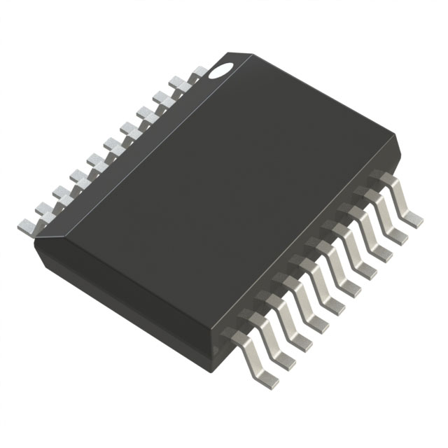
This ADN4655BRSZ belongs to Digital Isolators category. And its highest category level is Isolators. Digital Isolators category is subject to isolators. A mechanical switch known as an isolator isolates the substation's problematic area. In order to prevent the occurrence of serious flaws, this "ADN4655BRSZ" is used to divide a damaged area. A damaged area needs to be repaired from a healthy section. Analog Devices Inc. generates this ADN4655BRSZ. And it decides to upgrade this chip to meet consumers’ demand. Analog Devices Inc. is committed to be at the forefront of electronic component technology. The Tube is tailored to shape and size of the ADN4655BRSZ. The design of the ADN4655BRSZ packaging can keep the product from going bad and decrease costs. This electronic component’s applications involve high voltage devices such as transformers.

Tech Specifications

Maximum Differential Output Voltage (V)
Inputs - Side 1/Side 2
Differential Input High Threshold Voltage (V)
PPAP
Product Status
Automotive
Pulse Width Distortion (Max)
Supplier Package
Package / Case
Number of Channels
Technology
Voltage - Supply
REACH Status
Channel Type
Maximum Operating Supply Voltage (V)
EU RoHS
Moisture Sensitivity Level (MSL)
Operating Temperature
Voltage - Isolation
ECCN
Mounting Type
Standard Package Name
Pin Count
Mounting
Input Signal Type
Lead Shape
SVHC
Typical Operating Supply Voltage (V)
HTSUS
Package
Transmission Data Rate (Mbps)
Rise / Fall Time (Typ)
PCB changed
Common Mode Transient Immunity (Min)
HTS
ECCN (US)
Maximum Input Current (uA)
Supplier Device Package
Minimum Operating Temperature (°C)
Maximum Operating Temperature (°C)
Isolated Power
Function
Differential Input Low Threshold Voltage (V)
Data Rate
Package Height
Mfr
Propagation Delay tpLH / tpHL (Max)
RoHS Status
Maximum Propagation Delay Time (ns)
Package Length
Series
Type
Part Status
Package Width
Base Product Number
Minimum Operating Supply Voltage (V)
Maximum Rise Time
Isolation Type
RoHS
Supply Voltage - Min
Operating Supply Current
Development Kit
Polarity
Reverse Channels
Maximum Operating Temperature
Supply Voltage - Max
Forward Channels
Mounting Style
Isolation Voltage
Maximum Fall Time
Minimum Operating Temperature
Shutdown
Moisture Sensitive
Pd - Power Dissipation
USHTS
Propagation Delay Time

ADN4655BRSZ Documents

Download datasheets and manufacturer documentation for ADN4655BRSZ

Ersa ADN4654-56      

Shopping Guide

Payment Methods
Payment Methods include Prepayment TT (bank transfer), Western Union, and PayPal. Customers are responsible for shipping costs, bank charges, customs duties and taxes.
Shipping Rate
Shipments are made once a day around 5pm, excluding Sundays. Once shipped, the estimated delivery time is usually 5-7 business days, depending on the courier you choose.
Delivery Methods
Provide DHL, FedEx, UPS, EMS, SF Express and Registered Airmail International Delivery Service