
 German
 Japanese
 Portuguese
 Korea
Korea
 Mexico
 Dutch
Dutch


Analog Devices Inc.
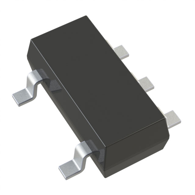
LTC6752HS5#TRMPBF

Why Choose Us?
Professional Platform
B2B & B2C purchasingDelivery at full speed
1-2 days deliveryWide variety
Original manufacturers365 days guarantee
Responsible quality
.png)


Tech Specifications
LTC6752HS5#TRMPBF Description
LTC6752HS5#TRMPBF Description
The LTC6752HS5#TRMPBF is a high-performance, general-purpose linear comparator offered by Analog Devices Inc., designed for a wide range of applications requiring precise voltage level detection and comparison. This device is currently active and compliant with REACH and RoHS3 standards, ensuring environmental and health safety. With a single element configuration, it operates within a supply voltage range of 2.45V to 3.5V, making it suitable for low-power applications.
LTC6752HS5#TRMPBF Features
- CMRR and PSRR: The LTC6752HS5#TRMPBF boasts a typical common-mode rejection ratio (CMRR) of 70dB and power supply rejection ratio (PSRR) of 73dB, ensuring high accuracy and stability in noisy environments.
- Output Type: The comparator features a CMOS output, which is ideal for driving capacitive loads and interfacing with digital systems.
- Output Current: It can source or sink up to 70mA, providing robust drive capability for various loads.
- Hysteresis: The 4.7mV hysteresis feature reduces the risk of output chatter and ensures reliable switching.
- Propagation Delay: With a maximum propagation delay of 5ns, the LTC6752HS5#TRMPBF offers fast response times.
- Input Offset Voltage: It has a maximum input offset voltage of 5.5mV at 3.3V, contributing to high precision in voltage comparisons.
- Quiescent Current: The maximum quiescent current is 5.8mA, which is low for energy-efficient operation.
- Input Bias Current: The maximum input bias current is 1.5µA at 3.3V, minimizing loading effects on the input signal source.
LTC6752HS5#TRMPBF Applications
The LTC6752HS5#TRMPBF is ideal for applications where precise voltage level detection and comparison are critical. Some specific use cases include:
- Industrial Control Systems: For monitoring and controlling voltage levels in industrial processes.
- Automotive Electronics: In battery management systems and sensor interfaces for reliable and accurate voltage monitoring.
- Medical Devices: For precise voltage detection in life-supporting and diagnostic equipment.
- Communication Systems: In signal detection and level restoration for reliable data transmission.
Conclusion of LTC6752HS5#TRMPBF
The LTC6752HS5#TRMPBF from Analog Devices Inc. stands out with its high CMRR and PSRR, low propagation delay, and robust output drive capability. Its CMOS output, hysteresis, and low power consumption make it a versatile choice for a variety of applications where reliable and precise voltage comparison is essential. The device's compliance with environmental standards and its fast response time further enhance its appeal in the electronics industry.
FAQ
| Quantity | Unit Price | Ext. Price |
|---|---|---|
| 1+ | $6.03680 | $6.04 |
| 10+ | $4.00752 | $40.08 |
| 25+ | $3.47776 | $86.94 |
| 100+ | $2.87848 | $287.85 |
| 250+ | $2.58431 | $646.08 |
Not available to buy online? Want the lower wholesale price? Please Send RFQ to get best price, we will respond immediately


.png?x-oss-process=image/format,webp/resize,h_32)


