
 German
 Japanese
 Portuguese
 Korea
Korea
 Mexico
 Dutch
Dutch



Fairchild (onsemi)
FIN210ACGFX


Why Choose Us?
Professional Platform
B2B & B2C purchasingDelivery at full speed
1-2 days deliveryWide variety
Original manufacturers365 days guarantee
Responsible quality

.png)



Tech Specifications
FIN210ACGFX Description
FIN210ACGFX Description
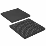
The FIN210ACGFX is a high-performance Serializer/Deserializer (SerDes) circuit designed by Fairchild Semiconductor, now part of onsemi. This telecom circuit is part of the µSerDes™ series and is packaged in a PBGA42 format. It features a robust LVCMOS and input output type, making it suitable for a wide range of digital communication applications. The device operates within a supply voltage range of 1.65V to 3.6V and supports a flexible number of inputs and outputs, with configurations of 10/2 and 2/10 respectively. It is designed for surface mount applications and is available in bulk packaging. The FIN210ACGFX is ROHS3 compliant, ensuring environmental sustainability and regulatory adherence. Despite its obsolete status, the FIN210ACGFX remains a reliable choice for legacy systems and specific applications where its unique features are required.
FIN210ACGFX Features
- LVCMOS Compatibility: The FIN210ACGFX features both LVCMOS input and output types, ensuring compatibility with a wide range of digital systems and simplifying integration into existing designs.
- Flexible I/O Configuration: With the ability to support 10 inputs and 2 outputs or 2 inputs and 10 outputs, the FIN210ACGFX offers versatile configurations to meet diverse application requirements.
- Wide Voltage Range: Operating within a supply voltage range of 1.65V to 3.6V, the device is adaptable to various power supply conditions, enhancing its usability across different environments.
- Surface Mount Technology: The surface mount mounting type facilitates efficient PCB design and manufacturing processes, reducing overall system size and improving reliability.
- ROHS3 Compliance: The FIN210ACGFX is ROHS3 compliant, ensuring it meets stringent environmental standards and regulatory requirements, making it suitable for global deployment.
- Bulk Packaging: Available in bulk packaging, the device is ideal for high-volume production and inventory management, offering cost-effective procurement options.
FIN210ACGFX Applications
The FIN210ACGFX is well-suited for applications requiring high-speed data transmission and efficient signal processing. Its unique features make it ideal for:
- Telecommunications: In telecom infrastructure, the FIN210ACGFX can be used for signal conversion and transmission, ensuring reliable and high-speed communication links.
- Data Centers: For data center applications, the device can facilitate efficient data routing and processing, enhancing overall system performance.
- Industrial Automation: In industrial settings, the FIN210ACGFX can be employed for real-time data transmission and control, supporting robust and reliable automation systems.
- Legacy Systems: Given its obsolete status, the FIN210ACGFX remains a critical component for maintaining and upgrading legacy systems where its specific features are still required.
Conclusion of FIN210ACGFX
The FIN210ACGFX, despite being obsolete, continues to offer significant value in specific applications due to its robust technical specifications and unique features. Its LVCMOS compatibility, flexible I/O configuration, and wide voltage range make it a versatile choice for various digital communication needs. The device's surface mount technology and ROHS3 compliance further enhance its appeal for modern electronics design and manufacturing. While newer alternatives may exist, the FIN210ACGFX remains a reliable option for legacy systems and specialized applications where its capabilities are unmatched.
FAQ
Not available to buy online? Want the lower wholesale price? Please Send RFQ to get best price, we will respond immediately










.png?x-oss-process=image/format,webp/resize,h_32)


