

Why Choose Us?
Professional Platform
B2B & B2C purchasingDelivery at full speed
1-2 days deliveryWide variety
Original manufacturers365 days guarantee
Responsible quality
.png)


Tech Specifications
CD4027BD3 Description
CD4027BD3 Description
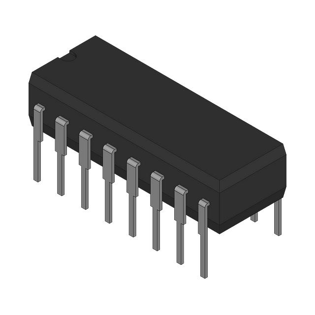
The CD4027BD3 is a dual J-K flip-flop logic IC chip manufactured by Harris Corporation. This chip is designed to provide robust performance in digital circuits, featuring a clock frequency of up to 24 MHz and a supply voltage range of 3V to 18V. It is equipped with complementary outputs and operates on a positive edge trigger mechanism. The CD4027BD3 is ideal for applications requiring set (preset) and reset functions, making it versatile for various digital logic designs. Despite its obsolescence, the CD4027BD3 remains a reliable choice for specific use cases where its unique features are advantageous.
CD4027BD3 Features
- Clock Frequency: Supports a maximum clock frequency of 24 MHz, ensuring high-speed operation.
- Output Type: Complementary outputs provide flexibility in circuit design.
- Trigger Type: Positive edge triggering ensures precise control and synchronization.
- Supply Voltage: Operates within a wide voltage range of 3V to 18V, offering compatibility with various power supplies.
- Low Quiescent Current: Consumes only 20 µA in quiescent state, making it energy-efficient.
- High Output Current: Capable of sourcing and sinking up to 6.8 mA, suitable for driving multiple loads.
- Low Propagation Delay: Achieves a maximum propagation delay of 90 ns at 15V and 50 pF, ensuring fast signal processing.
- Input Capacitance: Low input capacitance of 5 pF minimizes loading effects on driving circuits.
- Moisture Sensitivity Level: MSL 3 (168 Hours) indicates moderate sensitivity to moisture, suitable for standard manufacturing processes.
- Mounting Type: Through-hole mounting provides robust mechanical stability and ease of integration in PCB designs.
- Package: Available in bulk packaging, suitable for bulk purchasing and inventory management.
CD4027BD3 Applications
The CD4027BD3 is well-suited for a variety of applications due to its versatile features and performance capabilities. Some specific use cases include:
- Digital Counters: Ideal for constructing binary counters and frequency dividers.
- Sequential Logic Circuits: Suitable for designing state machines and other sequential logic systems.
- Data Storage and Transfer: Can be used in data latching and storage applications.
- Clock Management: Useful in clock signal processing and synchronization circuits.
- Control Logic: Applicable in control systems requiring precise timing and state management.
Conclusion of CD4027BD3
The CD4027BD3, despite being obsolete, continues to offer significant value in specific applications due to its unique features and performance benefits. Its wide supply voltage range, low quiescent current, and high output current make it suitable for a variety of digital circuits. The dual J-K flip-flop design with complementary outputs and positive edge triggering provides flexibility and precision in digital logic designs. While newer alternatives may exist, the CD4027BD3 remains a reliable choice for engineers and designers working with legacy systems or specific applications where its features are particularly advantageous.
FAQ
| Quantity | Unit Price | Ext. Price |
|---|---|---|
| 42+ | $6.32720 | $265.74 |
Not available to buy online? Want the lower wholesale price? Please Send RFQ to get best price, we will respond immediately


.png?x-oss-process=image/format,webp/resize,h_32)


