
 German
 Japanese
 Portuguese
 Korea
Korea
 Mexico
 Dutch
Dutch


Infineon Technologies
CY2303SXIT

Why Choose Us?
Professional Platform
B2B & B2C purchasingDelivery at full speed
1-2 days deliveryWide variety
Original manufacturers365 days guarantee
Responsible quality
.png)


Tech Specifications
CY2303SXIT Description
CY2303SXIT Description
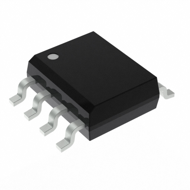
The CY2303SXIT is a clock multiplier and fanout distribution IC designed by Infineon Technologies. This obsolete yet highly capable device offers a range of features that make it suitable for various clock generation and distribution applications. It operates within a supply voltage range of 3V to 3.6V and supports LVCMOS and LVTTL input levels, providing LVCMOS output levels. The CY2303SXIT includes a Phase-Locked Loop (PLL) and is capable of multiplying the input clock frequency by a ratio of 1:3, achieving a maximum output frequency of 166.67MHz. The device is packaged in an 8-pin SOIC format and is available in a surface-mount configuration, making it ideal for compact designs. It is REACH unaffected and RoHS3 compliant, ensuring environmental sustainability and regulatory compliance.
CY2303SXIT Features
- Clock Multiplication and Distribution: The CY2303SXIT excels in generating and distributing clock signals with high precision and reliability. Its 1:3 multiplication ratio allows for efficient scaling of input frequencies, making it suitable for applications requiring higher clock rates.
- Wide Supply Voltage Range: Operating within a 3V to 3.6V supply voltage range, the CY2303SXIT provides flexibility in power supply options, ensuring compatibility with various system architectures.
- Input and Output Compatibility: The IC supports LVCMOS and LVTTL input levels and provides LVCMOS output levels, ensuring compatibility with a wide range of digital circuits and systems.
- Phase-Locked Loop (PLL): The inclusion of a PLL enhances the stability and accuracy of the clock signals, making the CY2303SXIT ideal for applications requiring precise timing.
- Surface-Mount Packaging: The 8-pin SOIC package and surface-mount configuration enable compact and efficient PCB designs, reducing footprint and improving thermal performance.
- Environmental Compliance: The CY2303SXIT is REACH unaffected and RoHS3 compliant, ensuring it meets stringent environmental and regulatory standards.
CY2303SXIT Applications
The CY2303SXIT is well-suited for a variety of applications where precise clock generation and distribution are critical. These include:
- Telecommunications: In base stations and communication equipment where stable and high-frequency clock signals are required.
- Networking: For switches, routers, and other networking devices that need reliable clock distribution.
- Consumer Electronics: In devices such as set-top boxes, digital TVs, and multimedia players where accurate timing is essential.
- Industrial Control Systems: For PLCs, automation systems, and other industrial applications requiring precise clock synchronization.
- Computing: In servers, workstations, and other computing devices where high-frequency clock signals are necessary for optimal performance.
Conclusion of CY2303SXIT
The CY2303SXIT is a robust and versatile clock multiplier and fanout distribution IC that offers a range of features and benefits tailored for high-performance applications. Despite its obsolete status, the device remains a reliable choice for systems requiring precise clock generation and distribution. Its wide supply voltage range, compatibility with LVCMOS and LVTTL levels, and inclusion of a PLL make it a standout option in its category. The CY2303SXIT's surface-mount packaging and environmental compliance further enhance its appeal for modern electronics designs.
FAQ
Not available to buy online? Want the lower wholesale price? Please Send RFQ to get best price, we will respond immediately


.png?x-oss-process=image/format,webp/resize,h_32)


