
 German
 Japanese
 Portuguese
 Korea
Korea
 Mexico
 Dutch
Dutch


Infineon Technologies
CY2308ESXI-1
Why Choose Us?
Professional Platform
B2B & B2C purchasingDelivery at full speed
1-2 days deliveryWide variety
Original manufacturers365 days guarantee
Responsible quality
.png)


Tech Specifications
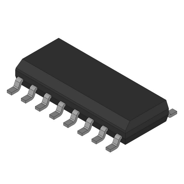
CY2308ESXI-1 Description
CY2308ESXI-1 Description
The CY2308ESXI-1 is a 3.3V Zero Delay Buffer designed by Cypress Semiconductor Corp, now part of Infineon Technologies. This device is categorized under Clock Generators & Support Products and is known for its high performance and reliability. The CY2308ESXI-1 features a 1:8 input-to-output ratio, making it ideal for applications requiring multiple clock outputs from a single input source. It supports LVCMOS and LVTTL input types and provides LVCMOS outputs, ensuring compatibility with a wide range of digital systems.
The CY2308ESXI-1 operates within a supply voltage range of 3V to 3.6V and can handle a maximum frequency of 100MHz. It includes a Phase-Locked Loop (PLL) with bypass capabilities, enhancing its flexibility and adaptability in various clock distribution scenarios. The device is available in a bulk package and is designed for surface mount applications, making it suitable for modern, compact electronic designs. Although the CY2308ESXI-1 is now considered obsolete, its robust design and performance continue to make it a reliable choice for specific applications.
CY2308ESXI-1 Features
- 1:8 Input-to-Output Ratio: The CY2308ESXI-1 efficiently distributes a single clock input to eight outputs, simplifying clock distribution in complex systems.
- LVCMOS and LVTTL Compatibility: The device supports both LVCMOS and LVTTL input types, ensuring broad compatibility with various digital systems.
- 3V to 3.6V Supply Voltage Range: This wide voltage range allows the CY2308ESXI-1 to operate in diverse power environments, enhancing its versatility.
- 100MHz Maximum Frequency: The CY2308XIES-1 can handle high-frequency clock signals up to 100MHz, making it suitable for high-speed applications.
- PLL with Bypass: The inclusion of a PLL with bypass capabilities provides flexibility in clock distribution and allows for precise control over clock signals.
- Surface Mount Design: The surface mount mounting type ensures compatibility with modern, compact PCB designs, facilitating easy integration into various electronic systems.
- Zero Delay Buffer: The zero delay feature ensures minimal latency in clock distribution, maintaining signal integrity and synchronization across multiple outputs.
CY2308ESXI-1 Applications
The CY2308XIES-1 is ideal for applications requiring precise clock distribution and synchronization. Its zero delay buffer and high-frequency capabilities make it suitable for:
- High-Speed Digital Systems: The CY2308ESXI-1 can effectively distribute clock signals in high-speed digital systems, ensuring synchronized operation of multiple components.
- Telecommunications: In telecommunication equipment, the device can provide reliable clock distribution for synchronization of data transmission and reception.
- Computer Systems: The CY2308ESXI-1 can be used in computer systems to distribute clock signals to various components, maintaining system performance and reliability.
- Industrial Control Systems: The robust design and wide voltage range make the CY2308ESXI-1 suitable for industrial control systems where precise timing and synchronization are crucial.
Conclusion of CY2308ESXI-1
The CY2308ESXI-1, despite being obsolete, remains a reliable choice for applications requiring precise clock distribution and synchronization. Its 1:8 input-to-output ratio, LVCMOS and LVTTL compatibility, and zero delay buffer features make it a versatile solution for high-speed digital systems, telecommunications, computer systems, and industrial control systems. The inclusion of a PLL with bypass capabilities further enhances its flexibility and adaptability. For systems where these features are essential, the CY2308ESXI-1 continues to offer a high-performance solution.
FAQ
| Quantity | Unit Price | Ext. Price |
|---|---|---|
| 100+ | $2.64000 | $264.00 |
Not available to buy online? Want the lower wholesale price? Please Send RFQ to get best price, we will respond immediately


.png?x-oss-process=image/format,webp/resize,h_32)


