
 German
 Japanese
 Portuguese
 Korea
Korea
 Mexico
 Dutch
Dutch


Infineon Technologies
CY23S08SI-2

Why Choose Us?
Professional Platform
B2B & B2C purchasingDelivery at full speed
1-2 days deliveryWide variety
Original manufacturers365 days guarantee
Responsible quality
.png)


Tech Specifications
CY23S08SI-2 Description
CY23S08SI-2 Description
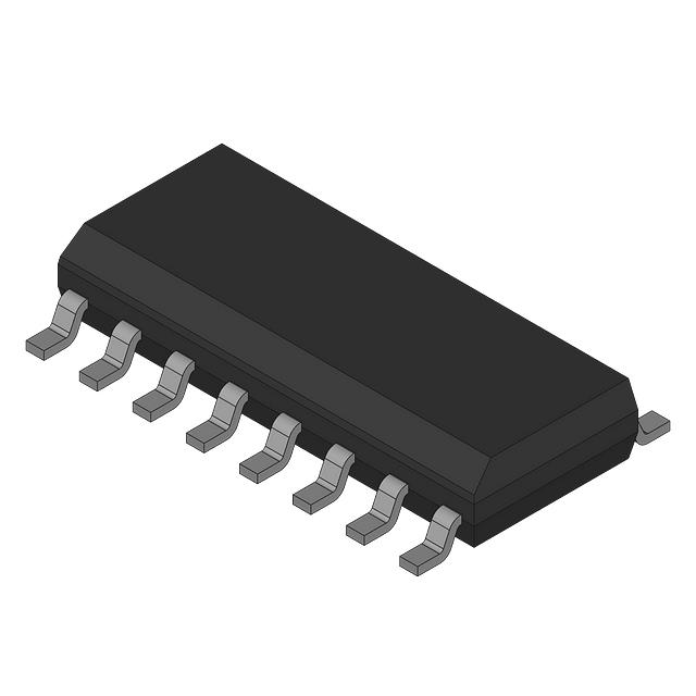
The CY23S08SI-2 is a high-performance clock buffer and zero delay buffer designed by Cypress Semiconductor Corp, a leading manufacturer in the electronics industry. This device is categorized under Clock/Timing ICs and is ideal for applications requiring precise clock signal distribution and synchronization. The CY23S08SI-2 features a 1:8 input-to-output ratio, making it suitable for applications where multiple clock signals need to be derived from a single input source. It supports LVCMOS and LVTTL input levels, ensuring compatibility with a wide range of digital systems. The output is designed to be LVCMOS, providing a clean and stable clock signal to downstream components. The device operates within a supply voltage range of 3V to 3.6V, making it suitable for low-power applications. It is available in a surface mount package, which is ideal for compact and high-density PCB designs. The CY23S08SI-2 is classified under ECCN EAR99 and HTSUS 8542.39.0001, indicating its compliance with international trade regulations. The product is REACH Affected, ensuring it meets environmental and safety standards. With a moisture sensitivity level (MSL) of 1 (Unlimited), the CY23S08SI-2 is suitable for a wide range of manufacturing environments without the need for special handling precautions.
CY23S08SI-2 Features
- Input-to-Output Ratio: The CY23S08SI-2 offers a 1:8 input-to-output ratio, allowing for efficient distribution of clock signals to multiple destinations from a single input source.
- Compatibility: Supports both LVCMOS and LVTTL input levels, ensuring compatibility with various digital systems and reducing the need for additional level-shifting components.
- Output Signal Quality: The LVCMOS output ensures clean and stable clock signals, minimizing jitter and improving overall system performance.
- Supply Voltage Range: Operates within a 3V to 3.6V supply voltage range, making it suitable for low-power applications and reducing power consumption.
- Mounting Type: Available in a surface mount package, ideal for compact and high-density PCB designs, enhancing space efficiency and reducing overall system size.
- Compliance: Classified under ECCN EAR99 and HTSUS 8542.39.0001, ensuring compliance with international trade regulations and facilitating global distribution.
- Environmental Standards: REACH Affected, ensuring the product meets environmental and safety standards, promoting sustainable and responsible manufacturing practices.
- Moisture Sensitivity: MSL 1 (Unlimited) rating allows for flexible manufacturing processes without the need for special handling precautions, reducing production complexity and costs.
CY23S08SI-2 Applications
The CY23S08SI-2 is ideal for a variety of applications where precise clock signal distribution and synchronization are critical. Some specific use cases include:
- Telecommunications: In base stations and communication equipment, where multiple clock signals are required for synchronization and timing control.
- Networking: In routers and switches, where reliable clock distribution is essential for maintaining data integrity and minimizing latency.
- Consumer Electronics: In devices such as smartphones, tablets, and smart TVs, where compact and low-power clock distribution solutions are necessary.
- Industrial Automation: In control systems and PLCs, where precise timing and synchronization are crucial for efficient operation and data processing.
- Medical Equipment: In diagnostic and monitoring devices, where accurate clock signals are essential for reliable performance and data accuracy.
Conclusion of CY23S08SI-2
The CY23S08SI-2 is a versatile and high-performance clock buffer and zero delay buffer that offers significant advantages over similar models. Its 1:8 input-to-output ratio, compatibility with LVCMOS and LVTTL input levels, and LVCMOS output ensure efficient and reliable clock signal distribution. The device's low-power operation, surface mount package, and compliance with international trade and environmental regulations make it an ideal choice for a wide range of applications. Whether used in telecommunications, networking, consumer electronics, industrial automation, or medical equipment, the CY23S08SI-2 provides a robust and reliable solution for precise clock signal distribution and synchronization.
FAQ
| Quantity | Unit Price | Ext. Price |
|---|---|---|
| 76+ | $3.47600 | $264.18 |
Not available to buy online? Want the lower wholesale price? Please Send RFQ to get best price, we will respond immediately


.png?x-oss-process=image/format,webp/resize,h_32)


