
 German
 Japanese
 Portuguese
 Korea
Korea
 Mexico
 Dutch
Dutch


Infineon Technologies
CY28341OC

Why Choose Us?
Professional Platform
B2B & B2C purchasingDelivery at full speed
1-2 days deliveryWide variety
Original manufacturers365 days guarantee
Responsible quality
.png)


Tech Specifications
CY28341OC Description
CY28341OC Description
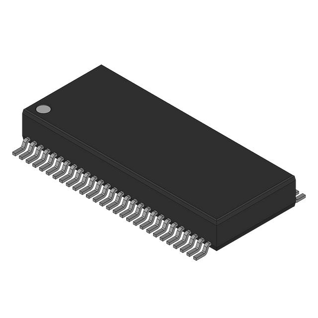
The CY28341OC is a high-performance clock/timing IC designed by Cypress Semiconductor Corp, specifically tailored for applications requiring precise and reliable clock signals. This device is ideal for DDR memory systems and is particularly well-suited for use with VIA P4 chipsets. The CY28341OC operates within a temperature range of 0°C to 70°C (TA) and is available in a surface-mount package, making it suitable for compact and high-density PCB designs.
CY28341OC Features
- Main Purpose: The primary function of the CY28341OC is to provide a stable and accurate clock signal for DDR memory systems, ensuring optimal performance and data integrity.
- Operating Temperature: With an operating temperature range of 0°C to 70°C (TA), the CY28341OC is designed for use in a variety of environments, from standard office conditions to more demanding industrial settings.
- PLL: The inclusion of a Phase-Locked Loop (PLL) ensures precise frequency control and stability, minimizing jitter and providing a clean clock signal.
- Input and Output: The device accepts a crystal input and provides a differential output, offering a 1:20 input-to-output ratio. This feature allows for efficient clock distribution and minimizes signal degradation.
- Voltage - Supply: The CY28341OC operates with a supply voltage range of 2.375V to 3.135V, providing flexibility in power supply design.
- Frequency - Max: Capable of generating clock signals up to a maximum frequency of 200MHz, the CY28341OC meets the high-speed requirements of modern DDR memory systems.
- Moisture Sensitivity Level (MSL): With an MSL of 3 (168 hours), the CY28341OC is suitable for standard manufacturing processes and ensures reliability during assembly.
CY28341OC Applications
The CY28341OC is particularly well-suited for applications that require high-speed, low-jitter clock signals. Its primary use case is in DDR memory systems, where it provides a stable clock signal to ensure reliable data transfer and memory performance. The device is also ideal for use with VIA P4 chipsets, where its differential output and precise frequency control offer significant performance benefits.
Conclusion of CY28341OC
The CY28341OC is a robust and reliable clock/timing IC that offers several unique features and advantages over similar models. Its high-frequency capability, differential output, and precise PLL control make it an excellent choice for DDR memory systems and VIA P4 chipsets. With its compact surface-mount package and wide operating temperature range, the CY28341OC is a versatile solution for a variety of electronic applications. Whether used in high-speed memory systems or other demanding applications, the CY28341OC ensures stable and accurate clock signals, enhancing overall system performance and reliability.
FAQ
Not available to buy online? Want the lower wholesale price? Please Send RFQ to get best price, we will respond immediately


.png?x-oss-process=image/format,webp/resize,h_32)


