
 German
 Japanese
 Portuguese
 Korea
Korea
 Mexico
 Dutch
Dutch


Infineon Technologies
CY29772AXI

Why Choose Us?
Professional Platform
B2B & B2C purchasingDelivery at full speed
1-2 days deliveryWide variety
Original manufacturers365 days guarantee
Responsible quality
.png)


Tech Specifications
CY29772AXI Description
CY29772AXI Description
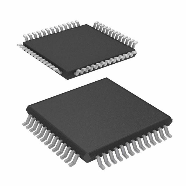
The CY29772AXI is an integrated circuit (IC) designed for fanout distribution, multiplexing, and zero-delay buffering applications. Manufactured by Infineon Technologies, this obsolete device is part of the Spread Aware™ series and is housed in a 52-pin TQFP package. It features a PLL with bypass capabilities and supports LVCMOS and crystal inputs. The supply voltage range is 2.375V to 3.465V, and the output is LVCMOS compatible. The device operates at a maximum frequency of 200MHz and has a 3:12 input-to-output ratio. It is REACH unaffected and ROHS3 compliant, with a moisture sensitivity level (MSL) of 3 (168 hours). The CY29772AXI is ideal for applications requiring high-frequency clock distribution and buffering.
CY29772AXI Features
- PLL with Bypass: The CY29772AXI includes a phase-locked loop (PLL) with bypass functionality, allowing for flexible clock generation and distribution. This feature ensures stable and accurate clock signals, crucial for high-performance systems.
- Wide Input Compatibility: The device supports both LVCMOS and crystal inputs, providing versatility in clock source options. This compatibility makes it suitable for various applications requiring different types of clock inputs.
- Supply Voltage Range: With a supply voltage range of 2.375V to 3.465V, the CY29772AXI is designed to operate efficiently within a broad voltage spectrum, ensuring compatibility with different power supply configurations.
- High-Frequency Operation: The CY29772AXI can operate at a maximum frequency of 200MHz, making it suitable for high-speed applications where precise clock distribution is essential.
- 3:12 Input-to-Output Ratio: The device features a 3:12 input-to-output ratio, enabling efficient fanout distribution and multiplexing of clock signals. This ratio is ideal for applications requiring multiple clock outputs from a single input.
- LVCMOS Output: The LVCMOS output ensures compatibility with a wide range of digital circuits, facilitating seamless integration into various electronic systems.
- Compliance and Reliability: The CY29772AXI is REACH unaffected and ROHS3 compliant, ensuring it meets environmental and safety standards. Additionally, its moisture sensitivity level (MSL) of 3 (168 hours) ensures reliability in various environmental conditions.
CY29772AXI Applications
The CY29772AXI is ideal for applications requiring high-frequency clock distribution and buffering. Some specific use cases include:
- Telecommunications: In high-speed communication systems, the CY29772AXI can provide stable clock signals for data transmission and reception, ensuring reliable performance.
- Networking: For networking equipment, the device can distribute clock signals to multiple components, maintaining synchronization across the system.
- Consumer Electronics: In devices such as routers, modems, and set-top boxes, the CY29772AXI can ensure accurate clock distribution, enhancing overall system performance.
- Industrial Automation: In industrial control systems, the CY29772AXI can provide precise clock signals for microcontrollers and other digital components, ensuring accurate timing and control.
Conclusion of CY29772AXI
The CY29772AXI is a versatile and reliable IC designed for high-frequency clock distribution and buffering applications. Its features, including a PLL with bypass, wide input compatibility, and high-frequency operation, make it suitable for various electronic systems. Although marked as obsolete, the CY29772AXI remains a valuable component for applications requiring precise clock distribution and buffering. Its compliance with environmental and safety standards ensures its continued use in modern electronic designs.
FAQ
Not available to buy online? Want the lower wholesale price? Please Send RFQ to get best price, we will respond immediately


.png?x-oss-process=image/format,webp/resize,h_32)


