
Infineon Technologies
CY2VC521ZXC-2
Clock Generators & Support Products


.png?x-oss-process=image/format,webp/resize,p_30)


CY2VC521ZXC-2 Description
CY2VC521ZXC-2 Description
The CY2VC521ZXC-2 is a zero delay buffer clock generator from Infineon Technologies, designed to provide high-performance clock distribution with minimal delay. This device is ideal for applications requiring precise timing and synchronization. It features a phase-locked loop (PLL) that ensures stable and accurate clock signal generation. The input is designed to accept a crystal oscillator, providing a reliable and low-jitter reference signal. The output is in LVDS format, which is suitable for high-speed and long-distance signal transmission.
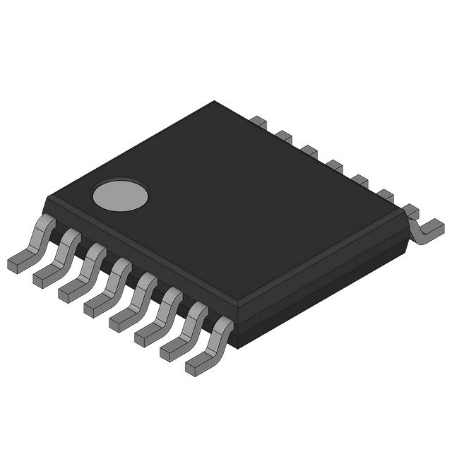
The CY2VC521ZXC-2 operates within a supply voltage range of 3.15V to 3.45V, making it suitable for low-power applications. It supports a maximum operating frequency of 216MHz, which is ideal for high-speed digital systems. The device is housed in a PDSO16 package and is designed for surface-mount applications, offering a compact and reliable solution for space-constrained designs.
CY2VC521ZXC-2 Features
- PLL Integration: The CY2VC521ZXC-2 incorporates a phase-locked loop (PLL) to ensure precise clock signal generation and synchronization.
- Crystal Input: The device accepts a crystal oscillator as the input reference, providing a stable and low-jitter clock source.
- LVDS Output: The LVDS output format allows for high-speed and long-distance signal transmission with minimal signal degradation.
- Wide Operating Frequency Range: With a maximum operating frequency of 216MHz, the CY2VC521ZXC-2 is suitable for high-speed digital systems.
- Low Power Consumption: The device operates within a supply voltage range of 3.15V to 3.45V, making it ideal for low-power applications.
- Surface Mount Compatibility: The PDSO16 package is designed for surface-mount applications, offering a compact and reliable solution for space-constrained designs.
- Compliance and Reliability: The CY2VC521ZXC-2 is REACH unaffected and RoHS3 compliant, ensuring environmental and safety standards are met. It also has a moisture sensitivity level (MSL) of 3, allowing for a 168-hour exposure before reflow soldering.
- Operating Temperature Range: The device operates reliably within a temperature range of 0°C to 70°C, making it suitable for a wide range of environmental conditions.
CY2VC521ZXC-2 Applications
The CY2VC521ZXC-2 is ideal for a variety of applications where precise clock distribution and synchronization are critical. Some specific use cases include:
- High-Speed Digital Systems: The high operating frequency and LVDS output make the CY2VC521ZXC-2 suitable for high-speed digital systems such as FPGAs, ASICs, and high-performance computing platforms.
- Telecommunications: The device's ability to provide stable and low-jitter clock signals makes it ideal for telecommunication applications, including base stations and network infrastructure.
- Industrial Automation: The CY2VC521ZXC-2 can be used in industrial automation systems where precise timing and synchronization are required for control and monitoring applications.
- Consumer Electronics: The compact PDSO16 package and surface-mount compatibility make the device suitable for consumer electronics, including smartphones, tablets, and gaming consoles.
Conclusion of CY2VC521ZXC-2
The CY2VC521ZXC-2 from Infineon Technologies is a high-performance zero delay buffer clock generator that offers precise timing and synchronization for a variety of applications. Its integrated PLL, crystal input, and LVDS output ensure stable and low-jitter clock signal generation. The device's wide operating frequency range, low power consumption, and compact surface-mount package make it an ideal solution for high-speed digital systems, telecommunications, industrial automation, and consumer electronics. The CY2VC521ZXC-2 is REACH unaffected, RoHS3 compliant, and has a moisture sensitivity level of 3, ensuring reliability and compliance with environmental and safety standards.
Tech Specifications
CY2VC521ZXC-2 Documents
Download datasheets and manufacturer documentation for CY2VC521ZXC-2
 CY2VC521-2
  Date Code/Shelf Life Chgs 18/Jul/2019 Ship Label REV
  CY2VC521-2
 Shopping Guide


.png?x-oss-process=image/format,webp/resize,h_32)


