
 German
 Japanese
 Portuguese
 Korea
Korea
 Mexico
 Dutch
Dutch


Infineon Technologies
CY7B991-2JXCT
Why Choose Us?
Professional Platform
B2B & B2C purchasingDelivery at full speed
1-2 days deliveryWide variety
Original manufacturers365 days guarantee
Responsible quality
.png)


Tech Specifications
CY7B991-2JXCT Description
CY7B991-2JXCT Description
The CY7B991-2JXCT is a high-performance clock buffer IC designed by Infineon Technologies, part of the RoboClock™ series. This device is specifically engineered to provide reliable and efficient clock signal distribution in various electronic systems. It features an 8:8 input-to-output ratio, ensuring that the input clock signal is accurately replicated across all output channels. The differential input and output capabilities enhance signal integrity, making it suitable for high-speed applications.
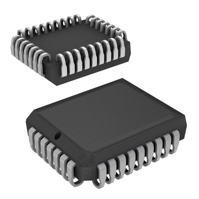
Operating within a temperature range of 0°C to 70°C, the CY7B991-2JXCT is designed for robust performance in typical industrial environments. It supports a supply voltage range of 4.5V to 5.5V, providing flexibility in power supply design. The device is packaged in a 32-pin PLCC (Plastic Leaded Chip Carrier) format, which is ideal for surface mount applications, ensuring ease of integration into modern PCB designs.
CY7B991-2JXCT Features
- High-Speed Performance: With a maximum operating frequency of 80 MHz, the CY7B991-2JXCT ensures precise and rapid clock signal distribution, making it suitable for high-speed digital systems.
- Differential Signaling: The differential input and output capabilities minimize signal degradation and electromagnetic interference (EMI), enhancing overall system performance.
- TTL Output: The TTL-compatible output ensures compatibility with a wide range of digital circuits, simplifying integration into existing systems.
- Robust Packaging: The 32PLCC package is designed for surface mount technology (SMT), providing mechanical stability and ease of assembly.
- Wide Operating Voltage Range: The 4.5V to 5.5V supply voltage range offers flexibility in power supply design, accommodating various power configurations.
- Compliance and Standards: The CY7B991-2JXCT is REACH unaffected and RoHS3 compliant, ensuring environmental safety and regulatory compliance.
CY7B991-2JXCT Applications
The CY7B991-2JXCT is ideal for a variety of applications where reliable clock signal distribution is critical. Some specific use cases include:
- Telecommunications: In base stations and network equipment, where high-speed clock signals are essential for data transmission and synchronization.
- Computing: In servers and high-performance computing systems, where precise clock distribution is required for optimal performance.
- Industrial Automation: In control systems and robotics, where reliable clock signals ensure accurate timing and coordination.
- Consumer Electronics: In devices such as gaming consoles and high-definition televisions, where high-speed clock signals are necessary for advanced processing and display capabilities.
Conclusion of CY7B991-2JXCT
The CY7B991-2JXCT is a versatile and high-performance clock buffer IC that offers significant advantages over similar models. Its differential signaling, wide operating voltage range, and high-speed performance make it an ideal choice for a variety of applications. Despite being marked as obsolete, the CY7B991-2JXCT remains a reliable option for designers seeking a robust clock distribution solution. Its compliance with industry standards and environmental regulations further enhances its appeal. For engineers and designers in need of a dependable clock buffer, the CY7B991-2JXCT is a proven and effective choice.
FAQ
Not available to buy online? Want the lower wholesale price? Please Send RFQ to get best price, we will respond immediately


.png?x-oss-process=image/format,webp/resize,h_32)


