
 German
 Japanese
 Portuguese
 Korea
Korea
 Mexico
 Dutch
Dutch



Infineon Technologies
CY7B9911-5JCT


Why Choose Us?
Professional Platform
B2B & B2C purchasingDelivery at full speed
1-2 days deliveryWide variety
Original manufacturers365 days guarantee
Responsible quality

.png)



Tech Specifications
CY7B9911-5JCT Description
CY7B9911-5JCT Description
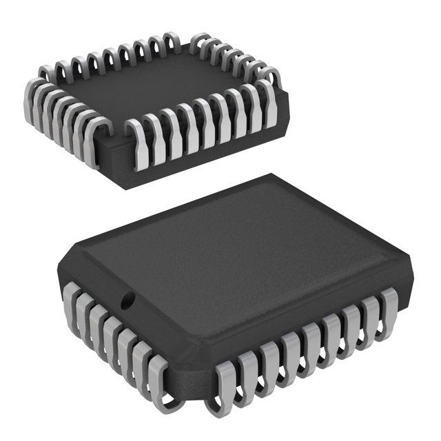
The CY7B9911-5JCT is a fanout buffer and zero delay buffer designed for high-performance clock distribution applications. Manufactured by Infineon Technologies, this IC is part of the RoboClock+™ series, known for its robustness and reliability in clock management solutions. The CY7B9911-5JCT operates within a supply voltage range of 4.5V to 5.5V and supports a maximum frequency of 100MHz. It features a 1:8 input-to-output ratio, making it suitable for applications requiring multiple clock signals derived from a single input. The device is designed for surface mount technology and comes in a 32PLCC package, ensuring ease of integration into modern electronic designs. Despite being marked as obsolete, the CY7B9911-5JCT remains a viable option for specific legacy systems and applications where its unique features are required.
CY7B9911-5JCT Features
- PLL Integration: The CY7B9911-5JCT incorporates a Phase-Locked Loop (PLL), enabling precise clock signal generation and synchronization.
- TTL Compatibility: Both input and output signals are TTL-compatible, ensuring seamless integration with a wide range of digital systems.
- Zero Delay Buffer: The device functions as a zero delay buffer, providing high precision and minimal jitter in clock signal distribution.
- Frequency Range: With a maximum operating frequency of 100MHz, the CY7B9911-5JCT is suitable for high-speed applications.
- Supply Voltage: The 4.5V to 5.5V supply voltage range offers flexibility in power supply design.
- Operating Temperature: The device operates reliably within a temperature range of 0°C to 70°C, making it suitable for various environmental conditions.
- Moisture Sensitivity Level (MSL): Rated at MSL 3 (168 hours), the CY7B9911-5JCT is designed to withstand typical manufacturing processes without degradation.
- REACH Compliance: The device is REACH unaffected, ensuring compliance with environmental and health regulations.
- ECCN and HTSUS: Classified under ECCN EAR99 and HTSUS 8542.39.0001, the CY7B9911-5JCT meets international trade and export control standards.
CY7B9911-5JCT Applications
The CY7B9911-5JCT is ideal for applications requiring precise clock distribution and synchronization. Its key use cases include:
- Telecommunications: Providing stable clock signals for communication equipment, ensuring reliable data transmission.
- Networking: Distributing clock signals across network devices to maintain synchronization and reduce jitter.
- Industrial Control Systems: Ensuring precise timing in automation and control systems, enhancing overall system reliability.
- Medical Equipment: Offering high-precision clock signals for medical devices where accurate timing is critical.
- Legacy Systems: Serving as a reliable component in older systems where its specific features are required to maintain functionality.
Conclusion of CY7B9911-5JCT
The CY7B9911-5JCT, despite being marked as obsolete, remains a valuable component for specific applications requiring high-precision clock distribution and synchronization. Its integration of a PLL, zero delay buffer functionality, and TTL compatibility make it a robust solution for a variety of electronic systems. While newer alternatives may exist, the CY7B9911-5JCT continues to offer reliable performance and is particularly suited for legacy systems and applications where its unique features are essential. For engineers and designers working with existing systems or requiring specific clock management capabilities, the CY7B9911-5JCT remains a viable and reliable choice.
FAQ
Not available to buy online? Want the lower wholesale price? Please Send RFQ to get best price, we will respond immediately




.png?x-oss-process=image/format,webp/resize,h_32)


