
 German
 Japanese
 Portuguese
 Korea
Korea
 Mexico
 Dutch
Dutch


Infineon Technologies
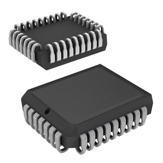
CY7B9911V-5JXC
Why Choose Us?
Professional Platform
B2B & B2C purchasingDelivery at full speed
1-2 days deliveryWide variety
Original manufacturers365 days guarantee
Responsible quality
.png)


Tech Specifications
CY7B9911V-5JXC Description
CY7B9911V-5JXC Description
The CY7B9911V-5JXC is a high-performance fanout buffer and zero-delay buffer designed by Infineon Technologies. This device is part of the clock generators and support products category, specifically tailored for applications requiring precise clock distribution and signal conditioning. The CY7B9911V-5JXC features a PLL (Phase-Locked Loop) and supports a wide operating voltage range of 3V to 3.6V, making it suitable for various power supply configurations. It operates within an industrial temperature range of 0°C to 70°C, ensuring reliability in diverse environmental conditions.
CY7B9911V-5JXC Features
- PLL Integration: The CY7B9911V-5JXC incorporates a PLL, which allows for precise clock synchronization and jitter reduction, essential for high-frequency applications.
- Input and Output Compatibility: The device supports LVTTL input and output levels, ensuring compatibility with a wide range of digital systems.
- Frequency Performance: With a maximum operating frequency of 110MHz, the CY7B9911V-5JXC is capable of handling high-speed clock signals, making it suitable for demanding applications.
- Fanout and Distribution: As a fanout buffer, it can distribute a single clock signal to multiple destinations without significant degradation, maintaining signal integrity.
- Zero-Delay Buffer: The zero-delay buffer feature ensures that the output clock signal is synchronized with the input, minimizing latency and improving system performance.
- Divider and Multiplier Capabilities: The device supports both clock division and multiplication, offering flexibility in generating various clock frequencies from a single input.
- Moisture Sensitivity Level: Rated at MSL 3 (168 hours), the CY7B9911V-5JXC is suitable for surface-mount assembly processes, ensuring robustness during manufacturing.
- Compliance: The CY7B9911V-5JXC meets REACH and RoHS3 compliance standards, ensuring environmental safety and regulatory adherence.
CY7B9911V-5JXC Applications
The CY7B9911V-5JXC is ideal for a variety of applications where high-frequency clock distribution and synchronization are critical. Some specific use cases include:
- Telecommunications: In base stations and communication equipment where precise clock distribution is necessary for maintaining signal integrity and minimizing latency.
- Data Centers: For distributing clock signals across multiple server components, ensuring synchronized operation and optimal performance.
- Industrial Automation: In systems requiring high-speed clock signals for real-time control and data processing.
- Consumer Electronics: In devices such as routers, switches, and other networking equipment where reliable clock distribution is essential.
Conclusion of CY7B9911V-5JXC
The CY7B9911V-5JXC from Infineon Technologies stands out as a versatile and high-performance solution for clock distribution and synchronization needs. Its integrated PLL, wide operating voltage range, and high-frequency capabilities make it a reliable choice for demanding applications. The device's compliance with industry standards and its robustness in various environmental conditions further enhance its appeal. While the product is marked as obsolete, its technical specifications and performance benefits continue to make it a valuable component for engineers and designers in the electronics industry.
FAQ
Not available to buy online? Want the lower wholesale price? Please Send RFQ to get best price, we will respond immediately


.png?x-oss-process=image/format,webp/resize,h_32)


