
 German
 Japanese
 Portuguese
 Korea
Korea
 Mexico
 Dutch
Dutch


Infineon Technologies
CY7B992-7JXC

Why Choose Us?
Professional Platform
B2B & B2C purchasingDelivery at full speed
1-2 days deliveryWide variety
Original manufacturers365 days guarantee
Responsible quality
.png)


Tech Specifications
CY7B992-7JXC Description
CY7B992-7JXC Description
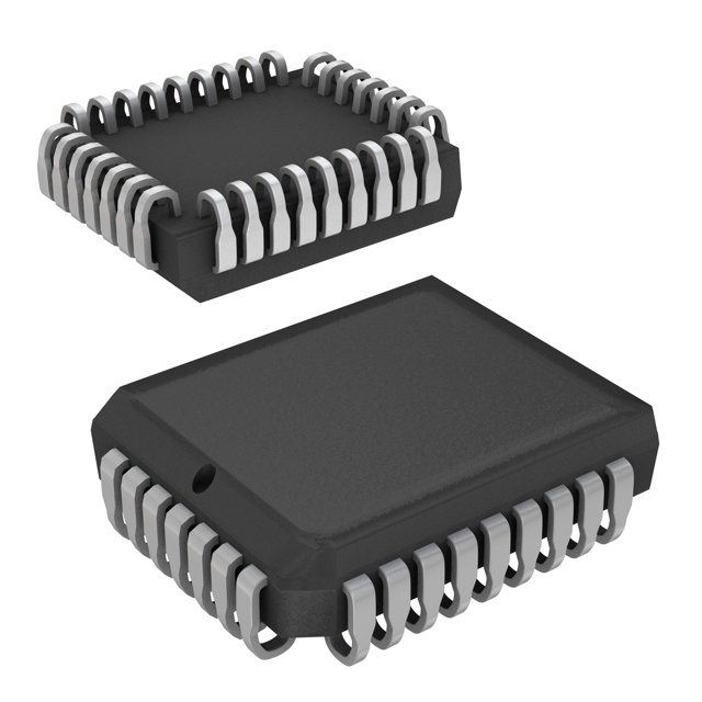
The CY7B992-7JXC is a fanout buffer/distribution and zero-delay buffer IC, designed by Infineon Technologies. This obsolete component is housed in a 32-lead plastic leaded chip carrier (PLCC) package and is suitable for surface mount applications. It operates within a supply voltage range of 4.5V to 5.5V and is designed to function within an operating temperature range of 0°C to 70°C. The CY7B992-7JXC supports CMOS input and output, making it compatible with a wide range of digital systems. It features a maximum operating frequency of 80MHz, providing high-speed performance for clock distribution and synchronization tasks.
CY7B992-7JXC Features
- PLL Integration: The CY7B992-7JXC includes a Phase-Locked Loop (PLL), which ensures precise clock signal generation and synchronization. This feature is essential for maintaining signal integrity and reducing jitter in high-speed digital systems.
- Frequency Range: With a maximum operating frequency of 80MHz, this IC is well-suited for applications requiring high-speed clock distribution.
- Input/Output Compatibility: The CMOS input and output compatibility make it easy to integrate with other digital components, ensuring seamless signal transmission.
- Supply Voltage Range: The 4.5V to 5.5V supply voltage range provides flexibility in power supply options, making it suitable for various power configurations.
- Operating Temperature: The 0°C to 70°C operating temperature range ensures reliable performance in typical industrial and commercial environments.
- Fanout and Zero-Delay Buffer: The CY7B992-7JXC functions as both a fanout buffer and a zero-delay buffer, providing efficient clock signal distribution and synchronization.
- Divider/Multiplier Capabilities: This IC supports both clock division and multiplication, offering additional flexibility in clock management.
- Compliance and Sensitivity: The CY7B992-7JXC is REACH unaffected and RoHS3 compliant, ensuring environmental and regulatory compliance. It also has a moisture sensitivity level (MSL) of 3, allowing for a 168-hour exposure time.
CY7B992-7JXC Applications
The CY7B992-7JXC is ideal for a variety of applications where precise clock signal distribution and synchronization are critical. Some specific use cases include:
- Telecommunications: In telecommunication systems, the CY7B992-7JXC can be used to distribute clock signals to multiple components, ensuring synchronized operation and reducing timing errors.
- Computing: In high-performance computing systems, this IC can help manage clock signals for processors, memory, and other peripherals, improving system performance and reliability.
- Industrial Control Systems: For industrial automation and control systems, the CY7B992-7JXC can provide stable clock signals to various components, ensuring accurate timing and control.
- Consumer Electronics: In consumer electronics, such as digital TVs and set-top boxes, the CY7B992-7JXC can be used to synchronize clock signals for video and audio processing.
Conclusion of CY7B992-7JXC
The CY7B992-7JXC is a versatile and reliable clock management IC, offering a combination of high-speed performance, precise synchronization, and flexible clock distribution capabilities. Its integration of a PLL, CMOS compatibility, and support for both fanout and zero-delay buffering make it a valuable component for a wide range of applications. Despite its obsolete status, the CY7B992-7JXC remains a robust solution for engineers and designers seeking high-performance clock management in their systems.
FAQ
| Quantity | Unit Price | Ext. Price |
|---|---|---|
| 6+ | $41.82640 | $250.96 |
Not available to buy online? Want the lower wholesale price? Please Send RFQ to get best price, we will respond immediately


.png?x-oss-process=image/format,webp/resize,h_32)


