
 German
 Japanese
 Portuguese
 Korea
Korea
 Mexico
 Dutch
Dutch


Infineon Technologies
S29GL064N90TFI040

Why Choose Us?
Professional Platform
B2B & B2C purchasingDelivery at full speed
1-2 days deliveryWide variety
Original manufacturers365 days guarantee
Responsible quality
.png)


Tech Specifications
S29GL064N90TFI040 Description
S29GL064N90TFI040
64Mbit (8MB) 3V Parallel NOR Flash | 90ns Access Time | Industrial Grade | TSOP-48
Density (8MB)
Access Time
Configurable Bus
Supply Range
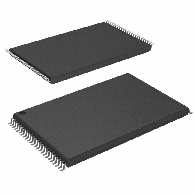
Package
Product Overview
The Infineon (formerly Cypress) S29GL064N90TFI040 is a 64Mbit (8,388,608 bytes) parallel NOR Flash memory from the GL‑N family, designed for embedded systems requiring high‑performance code execution, fast random access, and long‑term reliability. Operating from a standard 2.7V to 3.6V supply, it features a 90ns access time, enabling zero‑wait‑state operation with many microprocessors and microcontrollers. The device offers a flexible interface with configurable x16 or x8 data bus width, selectable via the BYTE# pin.
The S29GL064N is organized as 67 main sectors (64KB each) plus 8 parameter sectors (4KB each), providing fine‑granularity erase for boot code and parameter storage. Housed in a standard 48‑pin TSOP I package (TFI040 suffix), it operates over the industrial temperature range of -40°C to +85°C. The "040" suffix indicates a specific packing option (typically tray packaging). With 100,000 program/erase cycles and 20‑year data retention, this device is ideal for automotive aftermarket, industrial control, networking equipment, and telecom infrastructure.
📊 Technical Specifications
| Density / Organization | 64Mbit — 4M x16 / 8M x8 |
| Access Time (tACC) | 90ns max (random read) |
| Memory Interface | Parallel asynchronous (address/data multiplexed) |
| Supply Voltage (Vcc) | 2.7V – 3.6V |
| Operating Temperature | Industrial: -40°C to +85°C |
| Storage Temperature | -65°C to +150°C |
| Package Type | 48‑pin TSOP I (12x20mm, 0.5mm pitch) – TFI code |
| Package Dimensions | 12 x 20 x 1.0 mm |
| Sector Architecture | 67 main sectors (64KB each) + 8 parameter sectors (4KB each) |
| Endurance | 100,000 program/erase cycles (minimum) |
| Data Retention | 20 years (minimum) @ 55°C |
| Active Read Current | 20 mA (typical) |
| Standby Current | 100 µA (typical) |
| Write Protection | Hardware WP# pin, software block protection |
| Security Features | 64‑bit unique ID, 16‑byte OTP area |
| Program Time (Word/Byte) | 50 µs (typical) / 7 µs (typical) |
| Sector Erase Time | 0.5 s (typical, 64KB sector) |
| Chip Erase Time | 40 s (max) |
| RoHS / Halogen Free | Yes — “040” suffix indicates lead‑free, RoHS compliant |
| Moisture Sensitivity Level | MSL 3 (168 hours) |
| Part Status | Active — In production, longevity until 2030+ |
✨ Key Features
- ✅ Parallel NOR Flash – Fast 90ns access time for code execution, zero‑wait‑state with many MCUs/MPUs
- ✅ Configurable Bus Width – x16 (default) or x8 (via BYTE# pin) for flexible host interface
- ✅ Advanced Sector Protection – Individual sector lock/unlock for secure boot and data storage
- ✅ Banked Architecture – Partitioned into 4 banks for simultaneous operations (read while write/erase)
- ✅ Dual Operation Capability – Read from one bank while writing/erasing another, enabling non‑disruptive firmware updates
- ✅ Embedded Algorithms – Automatic program/erase operations with status register monitoring
- ✅ Hardware & Software Write Protection – WP# pin plus software‑controlled protection registers
- ✅ Automatic Sleep Mode – Lowers power consumption after 150ns of inactivity
- ✅ Unlock Bypass Mode – Accelerates programming for large data blocks (up to 32 words per cycle)
- ✅ Secured Silicon Region – 16‑byte factory‑programmed OTP area (some variants include 256‑bit secure ID)
- ✅ Common Flash Interface (CFI) – Provides standardized device information for software drivers
- ✅ Industrial Temperature Range – -40°C to +85°C for reliable operation in harsh environments
- ✅ Standard TSOP-48 Package – Easy board layout, pin‑compatible with many other parallel NOR devices
- ✅ Long‑term Availability – Infineon’s commitment to industrial and embedded markets (15+ years)
⚡ Parallel NOR Architecture & Read Performance
The S29GL064N is part of the GL family, which features a synchronous burst read mode (up to 33 MHz) and asynchronous page read mode (16‑word page), improving sustained read throughput for linear code execution.
🔒 Advanced Sector Protection & Security
🔐 Sector Locking
Each sector can be individually locked (write/erase protected) using the WP# pin and software control. The lock status can be programmed even when the WP# pin is active, providing flexible security.
🔑 Password‑Protected Program/Erase
Optional 64‑bit password protection prevents accidental or unauthorized write operations, ideal for secure boot code or configuration data.
📦 Secured Silicon Region (SSR)
A 16‑byte factory‑programmed OTP area (some variants include a 256‑bit secure ID) for permanent storage of unique serial numbers or encryption keys.
🛡️ Hardware Write Protection (WP#)
When WP# is driven low, the top or bottom sectors become write‑protected, safeguarding critical boot code without software intervention.
📦 Ordering Information & Part Number Decoder
| Orderable Part Number | Temperature | Package | Description |
|---|---|---|---|
| S29GL064N90TFI040 | -40°C to +85°C | TSOP-48 | Industrial, 90ns, tray (96 pcs/tray) |
| S29GL064N90TFI040 (TR) | -40°C to +85°C | TSOP-48 | Tape & Reel (1000 pcs/reel) |
| S29GL064N90TFI010 | -40°C to +85°C | TSOP-48 | Alternative ordering code, same spec |
| S29GL064N90TFI030 | -40°C to +85°C | TSOP-48 | Industrial, extended reliability |
• S29GL064N – Infineon (Cypress) GL‑N parallel NOR Flash family, 64Mbit
• 90 – Access time: 90ns
• T – Package: TSOP I (48‑pin)
• F – Industrial temperature range (-40°C to +85°C)
• I – Green, lead‑free, RoHS compliant
• 040 – Configuration / packing (tray, standard)
🏆 Infineon Technologies – Leading NOR Flash Manufacturer
Infineon Technologies (through its acquisition of Cypress Semiconductor) is a world‑leading supplier of NOR Flash memory, with a comprehensive portfolio of parallel and serial devices. The GL series (S29GLxxxN) is renowned for its reliability, long lifecycles, and support for industrial and automotive applications.
- Top 3 NOR Flash supplier worldwide – trusted by major OEMs
- AEC‑Q100 qualified automotive grade options available
- ISO 9001, ISO 14001, IATF 16949 certified manufacturing
- 65nm / 45nm NOR process nodes for high density and low power
- Long‑term product commitment – 15‑20 year availability for industrial and automotive programs
🛠️ Development Tools & Support
Infineon offers free samples, evaluation boards, and direct FAE support through authorized distributors. For automotive PPAP documentation, contact your local Infineon sales office.
📄 Certifications & Compliance
- RoHS 2011/65/EU (Compliant)
- REACH SVHC (Compliant)
- Halogen‑free per IEC 61249-2-21
- Conflict Minerals (CFSI) report available
- AEC‑Q100 Grade 2/3 options available
📦 Packaging & Logistics
- Tray: 96 pieces per tray (TSOP)
- Tape & Reel: 1000 pieces per 13" reel
- Moisture Sensitivity Level: MSL 3
- Lead finish: NiPdAu (green, lead‑free)
- Lead time: 8‑10 weeks ARO, stock via distributors
FAQ
Not available to buy online? Want the lower wholesale price? Please Send RFQ to get best price, we will respond immediately


.png?x-oss-process=image/format,webp/resize,h_32)


