
 German
 Japanese
 Portuguese
 Korea
Korea
 Mexico
 Dutch
Dutch


Intel
10M02DCU324C8G
696-10M02DCU324C8G

PDF Datasheet
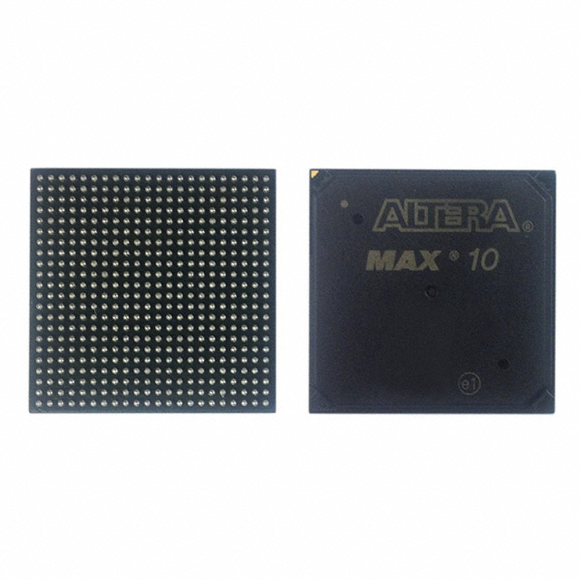
Field Programmable Gate Array, 2000-Cell, CMOS, PBGA324, 15 X 15 MM, 0.80 MM PITCH, ROHS COMPLIANT, UBGA-324
16 Weeks
Why Choose Us?
Professional Platform
B2B & B2C purchasingDelivery at full speed
1-2 days deliveryWide variety
Original manufacturers365 days guarantee
Responsible quality
.png)


Tech Specifications
Max Operating Temperature
85
Number of Terminals
324
Min Operating Temperature
0
Terminal Position
BOTTOM
JEDEC Package Code
S-PBGA-B324
Width
15
Length
15
Temperature Grade
OTHER
10M02DCU324C8G Description
MAX® 10 Field Programmable Gate Array (FPGA) IC 160 110592 2000 324-LFBGA
FAQ
What is 10M02DCU324C8G?
10M02DCU324C8G is a FPGAs from Intel. This product page provides its main specifications, pricing information, availability, and inquiry options.
What operating temperature range does 10M02DCU324C8G support?
Is 10M02DCU324C8G currently in stock?
What package or case is 10M02DCU324C8G available in?
Does 10M02DCU324C8G have quantity-based pricing?
Availability
(In Stock :
11 )
| Quantity | Unit Price | Ext. Price |
|---|---|---|
| 1+ | $21.11485 | $21.11 |
| 10+ | $20.45657 | $204.57 |
Quick Quote
ADD TO RFQ LIST
Not available to buy online? Want the lower wholesale price? Please Send RFQ to get best price, we will respond immediately
QUICK RFQ


.png?x-oss-process=image/format,webp/resize,h_32)


