
 German
 Japanese
 Portuguese
 Korea
Korea
 Mexico
 Dutch
Dutch


Intel
5CGXBC4C6F23C7N

Why Choose Us?
Professional Platform
B2B & B2C purchasingDelivery at full speed
1-2 days deliveryWide variety
Original manufacturers365 days guarantee
Responsible quality
.png)


Tech Specifications
5CGXBC4C6F23C7N Description
5CGXBC4C6F23C7N Description
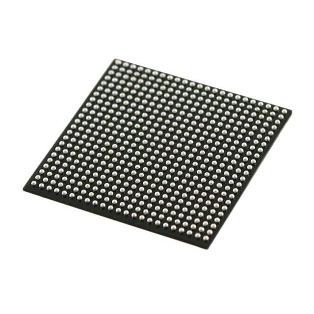
The 5CGXBC4C6F23C7N is a high-performance Field Programmable Gate Array (FPGA) from Intel, designed for demanding embedded applications. This FPGA belongs to the Cyclone® V GX series and is optimized for low power consumption and high performance. It features a robust architecture with 18,868 Logic Array Blocks (LABs) or Configurable Logic Blocks (CLBs), providing extensive programmability and flexibility. The device supports a wide operating temperature range of 0°C to 85°C (TJ), making it suitable for various industrial and commercial environments.
The 5CGXBC4C6F23C7N integrates 2,862,080 bits of total RAM, offering ample memory resources for complex computations and data storage. It also supports a supply voltage range of 1.07V to 1.13V, ensuring efficient power management and compatibility with modern low-power systems. The FPGA is housed in a 484-pin Fine Ball Grid Array (FBGA) package, which is ideal for surface mount applications and provides a compact footprint for space-constrained designs.
5CGXBC4C6F23C7N Features
- High Logic Capacity: With 50,000 logic elements/cells, the 5CGXBC4C6F23C7N can handle complex digital designs and algorithms, making it suitable for advanced signal processing and control applications.
- Extensive I/O Capability: The FPGA offers 240 I/O pins, providing ample connectivity options for interfacing with various peripherals and systems.
- Low Power Consumption: The operating voltage range of 1.07V to 1.13V ensures low power consumption, which is crucial for battery-powered and energy-efficient systems.
- Wide Operating Temperature Range: The 0°C to 85°C (TJ) operating temperature range makes the device suitable for a wide range of environmental conditions, enhancing its reliability and versatility.
- Moisture Sensitivity Level (MSL) 3: With an MSL of 3 (168 hours), the 5CGXBC4C6F23C7N is designed to withstand moisture exposure during manufacturing processes, ensuring high reliability and longevity.
- Compliance and Standards: The device is RoHS compliant and REACH unaffected, adhering to stringent environmental and safety regulations. It also carries an ECCN classification of 3A991D, ensuring compliance with export control regulations.
5CGXBC4C6F23C7N Applications
The 5CGXBC4C6F23C7N is ideal for a variety of embedded applications, including:
- Industrial Automation: The high logic capacity and extensive I/O capabilities make it suitable for complex control systems and real-time data processing in industrial environments.
- Communication Systems: The FPGA can be used in communication infrastructure for signal processing, protocol conversion, and data routing.
- Consumer Electronics: The low power consumption and compact form factor make it ideal for portable and energy-efficient consumer devices.
- Automotive Systems: The wide operating temperature range and robust design ensure reliability in automotive applications, such as advanced driver assistance systems (ADAS) and in-vehicle infotainment (IVI) systems.
- Medical Devices: The device's high performance and reliability make it suitable for medical imaging and diagnostic equipment, where precision and accuracy are critical.
Conclusion of 5CGXBC4C6F23C7N
The 5CGXBC4C6F23C7N FPGA from Intel is a versatile and high-performance solution for a wide range of embedded applications. Its extensive logic capacity, low power consumption, and robust design make it an ideal choice for demanding industrial, communication, and consumer applications. The device's compliance with environmental and safety standards ensures its suitability for global markets. With its advanced features and reliable performance, the 5CGXBC4C6F23C7N stands out as a superior choice for engineers and designers looking to implement complex digital systems.
FAQ
Not available to buy online? Want the lower wholesale price? Please Send RFQ to get best price, we will respond immediately


.png?x-oss-process=image/format,webp/resize,h_32)


