
 German
 Japanese
 Portuguese
 Korea
Korea
 Mexico
 Dutch
Dutch


Intel
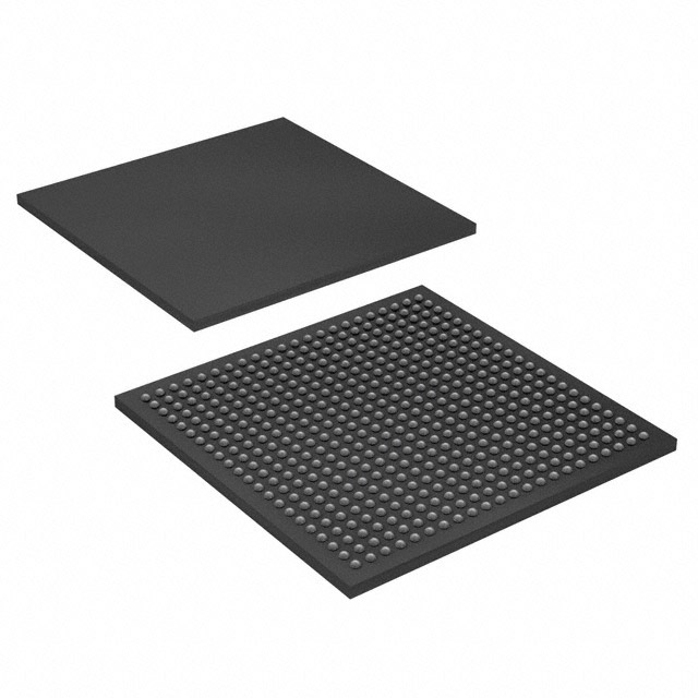
EP1S10F484C5

Why Choose Us?
Professional Platform
B2B & B2C purchasingDelivery at full speed
1-2 days deliveryWide variety
Original manufacturers365 days guarantee
Responsible quality
.png)


Tech Specifications
EP1S10F484C5 Description
The Intel EP1S10F484C5 is a high-performance, low-power FPGA (Field-Programmable Gate Array) device designed for a wide range of applications. This device is part of Intel's Cyclone V family of FPGAs, which are known for their high integration, low power consumption, and high performance.
Description:
The EP1S10F484C5 is a 484-pin FPGA device that offers a combination of high-density logic, memory, and I/O resources. It is based on Intel's low-power 28-nm process technology and features a high-speed transceiver for data rates up to 12.7 Gbps. The device also includes a range of advanced features such as hardened memory blocks, DSP blocks, and intellectual property (IP) cores.
Features:
- High-density logic resources: The EP1S10F484C5 offers a large number of logic elements (LEs) and flip-flops, making it suitable for complex digital designs.
- Memory resources: The device includes a range of memory resources, including block RAM (MLAB) and distributed RAM, to support data storage and processing requirements.
- High-speed transceivers: The EP1S10F484C5 features high-speed transceivers that support data rates up to 12.7 Gbps, making it suitable for high-speed data communication applications.
- Hardened memory blocks: The device includes hardened memory blocks for improved reliability and performance in memory-intensive applications.
- DSP blocks: The EP1S10F484C5 includes DSP blocks that provide high-performance, low-power digital signal processing capabilities.
- Intellectual property (IP) cores: The device supports a wide range of IP cores, including Ethernet, PCI Express, and DDR/DDR2/DDR3 memory controllers, making it easy to integrate with existing systems and protocols.
- Low power consumption: The EP1S10F484C5 is designed for low power consumption, making it suitable for battery-powered or energy-sensitive applications.
Applications:
The Intel EP1S10F484C5 FPGA device is suitable for a wide range of applications, including:
- Communications: The high-speed transceivers and Ethernet IP cores make the EP1S10F484C5 ideal for communication systems, such as network infrastructure, wireless base stations, and optical transport networks.
- Industrial automation: The device's robustness and low power consumption make it suitable for industrial automation and control systems, such as motor control, robotics, and machine vision.
- Automotive: The EP1S10F484C5 can be used in various automotive applications, including advanced driver assistance systems (ADAS), in-vehicle infotainment systems, and powertrain control.
- Medical electronics: The device's low power consumption and high reliability make it suitable for medical imaging systems, patient monitoring equipment, and other medical electronics.
- Defense and aerospace: The EP1S10F484C5 can be used in defense and aerospace applications, such as radar systems, satellite communications, and electronic warfare systems.
In summary, the Intel EP1S10F484C5 is a versatile, high-performance FPGA device that offers a range of features and capabilities suitable for various applications across different industries. Its combination of logic, memory, and I/O resources, along with advanced features such as hardened memory blocks and DSP blocks, make it an ideal choice for complex digital designs and high-speed data communication applications.
FAQ
Not available to buy online? Want the lower wholesale price? Please Send RFQ to get best price, we will respond immediately


.png?x-oss-process=image/format,webp/resize,h_32)


