

Intel
EP2S30F484C3
FPGAs

Not available to buy online? Want the lower wholesale price? Please Send RFQ to get best price, we will respond immediately


.png?x-oss-process=image/format,webp/resize,p_30)


EP2S30F484C3 Description
The Intel EP2S30F484C3 is a field programmable gate array (FPGA) device that belongs to the Cyclone II family of products. This device is designed to provide high performance and low power consumption, making it suitable for a wide range of applications.
Description:
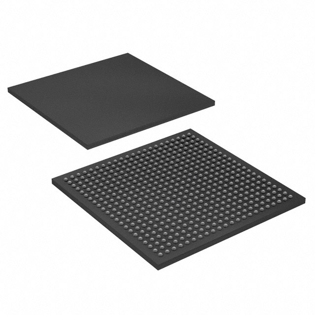
The EP2S30F484C3 is a mid-range FPGA device that offers a balance of performance and power efficiency. It features a high-density architecture and a rich set of programmable logic resources, making it ideal for a variety of applications. The device is available in a 484-pin flip-chip ball grid array (FCBGA) package.
Features:
- High-performance programmable logic: The EP2S30F484C3 features a high-performance programmable logic fabric that can be configured to implement a wide range of digital logic functions.
- Low power consumption: The device is designed to operate at low voltage levels, resulting in low power consumption and reduced heat dissipation.
- High-density architecture: The EP2S30F484C3 features a high-density architecture that allows for the implementation of complex designs in a compact form factor.
- Rich set of programmable logic resources: The device offers a wide range of programmable logic resources, including look-up tables (LUTs), flip-flops, and digital signal processing (DSP) blocks.
- On-chip memory: The EP2S30F484C3 includes a variety of on-chip memory resources, including block RAM and distributed RAM, to support data storage and processing requirements.
- High-speed I/O: The device features a high-speed I/O interface that supports data rates up to 1.2 Gbps, enabling high-speed data transfer between the FPGA and external devices.
- Configurable logic blocks: The EP2S30F484C3 includes configurable logic blocks that can be customized to meet specific design requirements.
Applications:
The Intel EP2S30F484C3 is suitable for a wide range of applications, including:
- Communications: The device can be used in communication systems, such as base stations, routers, and switches, to implement complex digital signal processing and network protocols.
- Industrial control: The EP2S30F484C3 can be used in industrial control systems to implement real-time control algorithms and manage input/output interfaces.
- Automotive: The device can be used in automotive applications, such as advanced driver assistance systems (ADAS) and infotainment systems, to implement complex processing and control functions.
- Consumer electronics: The EP2S30F484C3 can be used in consumer electronics, such as set-top boxes, gaming consoles, and digital cameras, to implement multimedia processing and user interface functions.
- Aerospace and defense: The device can be used in aerospace and defense applications, such as radar systems and satellite communications, to implement high-speed data processing and control functions.
In summary, the Intel EP2S30F484C3 is a versatile FPGA device that offers a balance of performance and power efficiency, making it suitable for a wide range of applications across various industries. Its high-density architecture, rich set of programmable logic resources, and high-speed I/O capabilities make it an ideal choice for complex digital designs.
Tech Specifications
EP2S30F484C3 Documents
Download datasheets and manufacturer documentation for EP2S30F484C3
Mult Dev Status Updates 29/May/2020 Mult Dev Status Rev 4/Dec/2020 Stratix II Device Handbook Mult Dev Label Chgs 24/Feb/2020 Mult Dev Label CHG 24/Jan/2020 Virtual JTAG Megafuntion Guide Mult Dev EOL 4/Dec/2020 Mult Dev Retraction 12/Feb/2021 Mult Series Software Chgs 26/Mar/2020 Related Parts


Shopping Guide


.png?x-oss-process=image/format,webp/resize,h_32)


©2025 ERSA Electronics Corporation.