

Intel
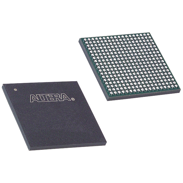
EP3C40F324I7
FPGAs

Not available to buy online? Want the lower wholesale price? Please Send RFQ to get best price, we will respond immediately


.png?x-oss-process=image/format,webp/resize,p_30)


EP3C40F324I7 Description
The Intel EP3C40F324I7 is a high-performance field programmable gate array (FPGA) that is part of Intel's Cyclone III family. This FPGA is designed to provide high-density, low-power, and cost-effective solutions for a wide range of applications.
Description:
The EP3C40F324I7 is a mid-range FPGA that features a high-density of programmable logic elements and a rich set of I/O resources. It has a total of 33,792 logic elements, 288 dedicated multipliers, and 1,152 single data rate (SDR) RAM blocks. The device also has a high-speed transceiver that supports data rates up to 3.5 Gbps, making it suitable for high-speed communication applications.
Features:
Some of the key features of the EP3C40F324I7 include:
- High-density programmable logic elements: The FPGA has a large number of programmable logic elements that can be configured to implement a wide range of digital logic functions.
- Dedicated multipliers: The device has 288 dedicated multipliers that can be used for high-speed arithmetic operations.
- Single data rate (SDR) RAM blocks: The FPGA has 1,152 SDR RAM blocks that can be used for data storage and processing.
- High-speed transceiver: The device has a high-speed transceiver that supports data rates up to 3.5 Gbps, making it suitable for high-speed communication applications.
- Low power consumption: The Cyclone III family of FPGAs is designed to have low power consumption, making it suitable for battery-powered and energy-efficient applications.
- Robust I/O resources: The FPGA has a rich set of I/O resources, including differential I/Os, high-speed LVDS, and multi-purpose clock pins.
Applications:
The EP3C40F324I7 is suitable for a wide range of applications, including:
- Communications: The high-speed transceiver and dedicated multipliers make the FPGA well-suited for high-speed communication applications, such as 10G Ethernet and 4G/5G wireless infrastructure.
- Signal processing: The FPGA's high-density of programmable logic elements and dedicated multipliers make it ideal for signal processing applications, such as image and video processing, radar signal processing, and medical imaging.
- Industrial control: The FPGA's robust I/O resources and low power consumption make it suitable for industrial control applications, such as motor control, robotics, and factory automation.
- Automotive: The device's low power consumption and high reliability make it suitable for automotive applications, such as advanced driver assistance systems (ADAS), infotainment systems, and body control modules.
- Consumer electronics: The FPGA's versatility and low power consumption make it suitable for consumer electronics applications, such as set-top boxes, gaming consoles, and smart home devices.
In summary, the Intel EP3C40F324I7 is a high-performance FPGA that offers a combination of high-density programmable logic elements, dedicated multipliers, and robust I/O resources. Its low power consumption and high-speed transceiver make it suitable for a wide range of applications, including communications, signal processing, industrial control, automotive, and consumer electronics.
Tech Specifications
EP3C40F324I7 Documents
Download datasheets and manufacturer documentation for EP3C40F324I7
Cyclone III_Design Guidelines Cyclone III Device Handbook Vol1 Cyclone III Family Overview Mult Dev Label Chgs 24/Feb/2020 Mult Dev Label CHG 24/Jan/2020 Virtual JTAG Megafuntion Guide Cyclone III Device Handbook Vol1 Mult Series Software Chgs 26/Mar/2020 Mult PN LABEL 01/08/2023 Related Parts


Shopping Guide


.png?x-oss-process=image/format,webp/resize,h_32)


©2025 ERSA Electronics Corporation.