
Intel
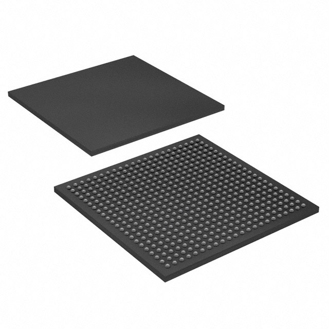
EP3SL50F484C3N
FPGAs


.png?x-oss-process=image/format,webp/resize,p_30)


EP3SL50F484C3N Description
The Intel EP3SL50F484C3N is a high-performance, low-power FPGA (Field-Programmable Gate Array) device designed for a wide range of applications. This device is part of Intel's Cyclone V family, which is known for its low power consumption, high performance, and versatility.
Description:
The EP3SL50F484C3N is a compact and powerful FPGA device that offers a combination of features and capabilities suitable for various applications. It is based on a 28 nm low-power process technology and features a high-density architecture, making it an ideal choice for complex and power-sensitive designs.
Features:
- Low Power Consumption: The device is designed to operate at low power levels, making it suitable for battery-powered and energy-efficient applications.
- High Performance: The EP3SL50F484C3N offers high-speed performance, with support for high-frequency clocking and fast I/O capabilities.
- Versatile I/O Options: The device provides a wide range of I/O options, including LVCMOS, LVDS, and DDR interfaces, allowing for easy integration with various peripherals and systems.
- On-chip Memory: The FPGA features a large amount of on-chip memory resources, including block RAM and distributed RAM, which can be used for data storage and processing tasks.
- Digital Signal Processing (DSP) Capabilities: The EP3SL50F484C3N includes dedicated DSP blocks, which can be used for high-speed mathematical and signal processing tasks.
- Security Features: The device offers advanced security features, such as encryption and authentication, to protect sensitive data and intellectual property.
- Configuration and Debugging Support: The FPGA provides support for configuration and debugging through JTAG and other interfaces, making it easier to develop and test designs.
Applications:
The Intel EP3SL50F484C3N is suitable for a wide range of applications, including but not limited to:
- Industrial Automation: The device can be used in control systems, motor drives, and sensor interfaces for industrial automation applications.
- Consumer Electronics: The low power consumption and high performance make it suitable for use in consumer electronics, such as smartphones, tablets, and wearable devices.
- Automotive: The FPGA can be used in various automotive applications, including infotainment systems, advanced driver assistance systems (ADAS), and body control modules.
- Communications: The device is suitable for communication systems, such as base stations, routers, and switches, due to its high-speed performance and versatile I/O options.
- Medical Electronics: The EP3SL50F484C3N can be used in medical imaging systems, patient monitoring devices, and other medical electronics that require high performance and low power consumption.
- Aerospace and Defense: The FPGA is suitable for aerospace and defense applications, such as radar systems, satellite communications, and secure communication devices.
In summary, the Intel EP3SL50F484C3N is a versatile, high-performance, and low-power FPGA device that offers a wide range of features and capabilities, making it suitable for various applications across different industries.
Tech Specifications
EP3SL50F484C3N Documents
Download datasheets and manufacturer documentation for EP3SL50F484C3N
 Stratix III Device Family Overview Stratix III Device Handbook
  Mult Dev Label Chgs 24/Feb/2020 Mult Dev Label CHG 24/Jan/2020
  Virtual JTAG Megafuntion Guide
  Readiness Plan Update 3/Apr/2020
  Mult Dev EOL REV 2/Aug/2019 Mult Dev EOL 28/Feb/2019 Mult Dev Add Subs 6/Sep/2019
  Mult Series Software Chgs 26/Mar/2020
 Shopping Guide


.png?x-oss-process=image/format,webp/resize,h_32)


