

Lattice Semiconductor
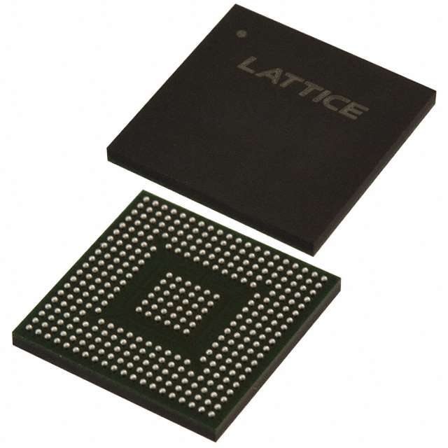
LCMXO2-4000HC-5BG332C
FPGAs

Not available to buy online? Want the lower wholesale price? Please Send RFQ to get best price, we will respond immediately


.png?x-oss-process=image/format,webp/resize,p_30)


LCMXO2-4000HC-5BG332C Description
The LCMXO2-4000HC-5BG332C is a high-performance field programmable gate array (FPGA) from Lattice Semiconductor. This device is part of the LatticeMico series of FPGAs, which are designed for high-density and low-power applications.
Description:
The LCMXO2-4000HC-5BG332C is a mid-range FPGA that offers a balance of performance, power efficiency, and cost. It is based on Lattice's 28 nm low-power process technology and features a high-speed transceiver for data rates up to 5 Gbps. The device has a configurable logic block architecture that allows for flexible and customizable designs.
Features:
Some of the key features of the LCMXO2-4000HC-5BG332C include:
- 28 nm low-power process technology
- High-speed transceiver for data rates up to 5 Gbps
- Configurable logic block architecture
- Advanced DSP blocks for high-performance signal processing
- Integrated memory resources for high-density storage
- Low-power design for extended battery life in portable applications
- Security features for protecting intellectual property and data
Applications:
The LCMXO2-4000HC-5BG332C is suitable for a wide range of applications, including:
- Communications infrastructure, such as routers, switches, and network interface cards
- Industrial control systems, including motor control and machine vision
- Automotive applications, such as advanced driver assistance systems (ADAS) and infotainment systems
- Consumer electronics, including smart home devices and wearable technology
- Aerospace and defense applications, such as radar and electronic warfare systems
- Medical devices, such as imaging systems and patient monitoring equipment
In summary, the LCMXO2-4000HC-5BG332C is a versatile and powerful FPGA that offers a range of features and benefits for various applications. Its low-power design, high-performance capabilities, and flexible architecture make it an ideal choice for designers looking to create innovative and efficient solutions.
Tech Specifications
LCMXO2-4000HC-5BG332C Documents
Download datasheets and manufacturer documentation for LCMXO2-4000HC-5BG332C
Alternate Assembly/Test Site 06/Oct/2014 MachXO2 Family Datasheet MachXO2 Family Handbook Product Selector Guide All Dev Pkg Mark Chg 12/Nov/2018 I2C Read-Back Failure Feb/2015 MachXO2 Family Handbook MachXO2™ Family Datasheet Datasheet Chg 21/Mar/2016 Top Mark Format Change 20/Dec/2023 Related Parts


Relevant Search
Shopping Guide


.png?x-oss-process=image/format,webp/resize,h_32)


©2025 ERSA Electronics Corporation.