
 German
 Japanese
 Portuguese
 Korea
Korea
 Mexico
 Dutch
Dutch


Lattice Semiconductor
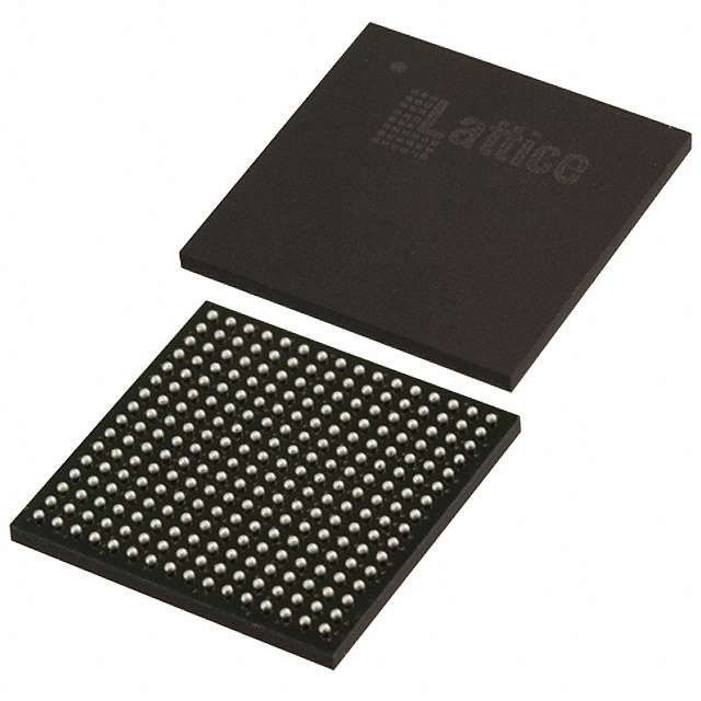
LCMXO2-4000HC-6FTG256I

Why Choose Us?
Professional Platform
B2B & B2C purchasingDelivery at full speed
1-2 days deliveryWide variety
Original manufacturers365 days guarantee
Responsible quality
.png)


Tech Specifications
LCMXO2-4000HC-6FTG256I Description
The Lattice Semiconductor's LCMXO2-4000HC-6FTG256I is a high-performance field programmable gate array (FPGA) device that offers a wide range of features and applications.
Description:
The LCMXO2-4000HC-6FTG256I is a member of Lattice Semiconductor's low-cost, low-power, and small form factor FPGA family. It is designed to provide high performance and flexibility for a variety of applications, including communications, industrial, and consumer electronics.
Features:
- High-performance programmable logic: The LCMXO2-4000HC-6FTG256I features a high-performance programmable logic fabric that can be configured to implement a wide range of digital logic functions.
- Low power consumption: The device is designed to operate with low power consumption, making it ideal for battery-powered and energy-sensitive applications.
- Small form factor: The LCMXO2-4000HC-6FTG256I is available in a compact 6FTG256I package, making it suitable for space-constrained applications.
- High-speed transceivers: The device includes high-speed transceivers that support data rates up to 12.5 Gbps, making it suitable for high-speed communication applications.
- Integrated memory: The LCMXO2-4000HC-6FTG256I includes integrated memory resources, including block RAM and distributed RAM, that can be used to store data and implement complex logic functions.
- Configurable I/O: The device features a wide range of configurable I/O options, including LVCMOS, LVDS, and serdes, making it suitable for a variety of interface requirements.
Applications:
The LCMXO2-4000HC-6FTG256I is suitable for a wide range of applications, including:
- Communications: The high-speed transceivers and low power consumption make the LCMXO2-4000HC-6FTG256I ideal for communication applications, such as wireless base stations, network infrastructure, and optical transport networks.
- Industrial: The device's small form factor and configurable I/O options make it suitable for industrial applications, such as motor control, machine vision, and process automation.
- Consumer electronics: The LCMXO2-4000HC-6FTG256I can be used in consumer electronics applications, such as smart home devices, wearables, and gaming consoles.
- Automotive: The device's reliability and robustness make it suitable for automotive applications, such as infotainment systems, advanced driver assistance systems (ADAS), and body control modules.
- Aerospace and defense: The LCMXO2-4000HC-6FTG256I can be used in aerospace and defense applications, such as satellite communications, radar systems, and secure communication systems.
Overall, the Lattice Semiconductor's LCMXO2-4000HC-6FTG256I is a versatile and powerful FPGA device that offers a wide range of features and applications, making it an excellent choice for a variety of projects and industries.
FAQ
Not available to buy online? Want the lower wholesale price? Please Send RFQ to get best price, we will respond immediately


.png?x-oss-process=image/format,webp/resize,h_32)


