
 German
 Japanese
 Portuguese
 Korea
Korea
 Mexico
 Dutch
Dutch



Lattice Semiconductor
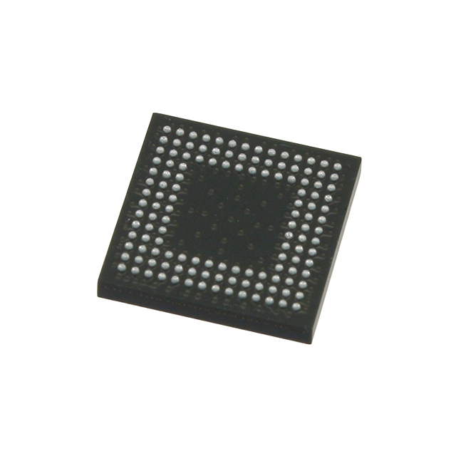
LCMXO2-4000HE-6MG132I


Why Choose Us?
Professional Platform
B2B & B2C purchasingDelivery at full speed
1-2 days deliveryWide variety
Original manufacturers365 days guarantee
Responsible quality

.png)



Tech Specifications
LCMXO2-4000HE-6MG132I Description
The LCMXO2-4000HE-6MG132I is a field programmable gate array (FPGA) device manufactured by Lattice Semiconductor. This device is part of the LatticeECP2M family of FPGAs, which are designed for high-performance and low-power applications.
Description:
The LCMXO2-4000HE-6MG132I is a high-density FPGA with a programmable logic array consisting of 4000 logic elements. It features a 6-layer metal over glass package with a total of 132 I/O pins. The device operates at a maximum frequency of 1 GHz and has a low standby power consumption of less than 30 mW.
Features:
- High-density programmable logic array with 4000 logic elements.
- 6-layer metal over glass package with 132 I/O pins.
- Maximum operating frequency of 1 GHz.
- Low standby power consumption of less than 30 mW.
- Configurable I/O interface supporting various protocols and standards.
- On-chip memory resources, including block RAM and distributed RAM.
- Integrated digital signal processing (DSP) blocks for high-performance data processing.
- Security features, including encryption and authentication.
Applications:
The LCMXO2-4000HE-6MG132I FPGA is suitable for a wide range of applications, including:
- Communications infrastructure, such as 5G base stations and optical transport networks.
- Industrial control systems, including motor control and factory automation.
- Automotive applications, such as advanced driver assistance systems (ADAS) and infotainment systems.
- Consumer electronics, including smart home devices and wearable technology.
- Aerospace and defense applications, including radar and electronic warfare systems.
- High-performance computing and data processing systems.
In summary, the LCMXO2-4000HE-6MG132I is a high-performance, low-power FPGA that offers a wide range of features and applications. Its high-density programmable logic array, configurable I/O interface, and on-chip memory resources make it an ideal choice for various applications, from communications infrastructure to consumer electronics.
FAQ
Not available to buy online? Want the lower wholesale price? Please Send RFQ to get best price, we will respond immediately






.png?x-oss-process=image/format,webp/resize,h_32)


