
 German
 Japanese
 Portuguese
 Korea
Korea
 Mexico
 Dutch
Dutch


Lattice Semiconductor
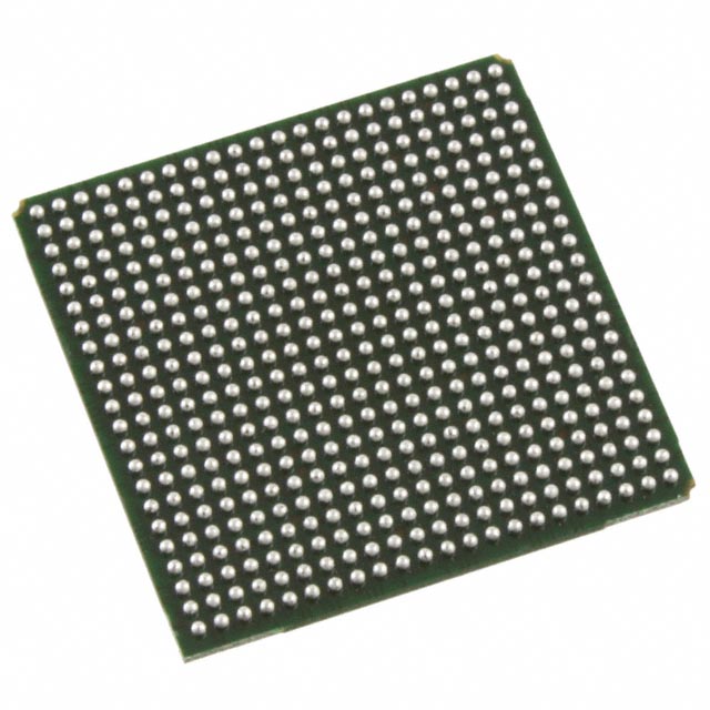
LFE2-50E-5FN484C

Why Choose Us?
Professional Platform
B2B & B2C purchasingDelivery at full speed
1-2 days deliveryWide variety
Original manufacturers365 days guarantee
Responsible quality
.png)


Tech Specifications
LFE2-50E-5FN484C Description
Lattice Semiconductor's LFE2-50E-5FN484C is a high-performance programmable logic device designed for a wide range of applications. This device is part of the LatticeECP2 family, which offers a combination of low power consumption, high performance, and small form factor.
Description:
The LFE2-50E-5FN484C is a 5.0 V FPGA (Field-Programmable Gate Array) that comes in a 484-pin FBGA package. It features a high-density architecture, making it suitable for complex and demanding applications.
Features:
- Low power consumption: The LFE2-50E-5FN484C is designed to operate with low power consumption, making it ideal for battery-powered or energy-sensitive applications.
- High performance: With its high-speed processing capabilities, the LFE2-50E-5FN484C can handle complex tasks and data-intensive applications with ease.
- Small form factor: The 484-pin FBGA package allows for a compact design, making it suitable for applications with space constraints.
- Versatility: The programmable nature of the LFE2-50E-5FN484C allows it to be customized for a wide range of applications, providing flexibility in design and implementation.
- Robust design: Lattice Semiconductor is known for its high-quality products, and the LFE2-50E-5FN484C is no exception. It is built to withstand various environmental conditions and provide reliable performance.
Applications:
The LFE2-50E-5FN484C is suitable for a wide range of applications, including but not limited to:
- Industrial automation: The device can be used in control systems, motor drives, and sensor interfaces for industrial applications.
- Communications: The high-speed processing capabilities make it suitable for communication systems, such as network infrastructure, routers, and switches.
- Consumer electronics: The LFE2-50E-5FN484C can be used in various consumer electronics, such as set-top boxes, gaming consoles, and smart home devices.
- Automotive: The device can be employed in automotive applications, such as infotainment systems, advanced driver assistance systems (ADAS), and battery management systems.
- Aerospace and defense: The LFE2-50E-5FN484C can be utilized in aerospace and defense applications, such as navigation systems, radar processing, and secure communication systems.
In summary, Lattice Semiconductor's LFE2-50E-5FN484C is a versatile, high-performance FPGA that offers low power consumption and a small form factor. It is suitable for a wide range of applications, from industrial automation to consumer electronics, making it an excellent choice for designers looking for a reliable and adaptable solution.
FAQ
Not available to buy online? Want the lower wholesale price? Please Send RFQ to get best price, we will respond immediately


.png?x-oss-process=image/format,webp/resize,h_32)


