
 German
 Japanese
 Portuguese
 Korea
Korea
 Mexico
 Dutch
Dutch


Lattice Semiconductor
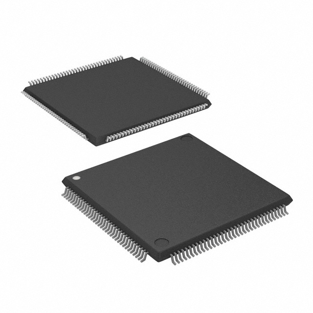
LFE2-6E-6T144C

Why Choose Us?
Professional Platform
B2B & B2C purchasingDelivery at full speed
1-2 days deliveryWide variety
Original manufacturers365 days guarantee
Responsible quality
.png)


Tech Specifications
LFE2-6E-6T144C Description
Lattice Semiconductor's LFE2-6E-6T144C is a field programmable gate array (FPGA) device that is part of the company's low-cost, low-power EC family of products. This device is designed to provide a cost-effective solution for a wide range of applications, including embedded systems, communications, and industrial control.
Description:
The LFE2-6E-6T144C is an enhanced version of Lattice's original LFE2E device, offering improved performance, reduced power consumption, and increased functionality. It features a 6-input lookup table (LUT) architecture, which allows for high-density logic implementation and fast switching speeds.
Features:
- Low power consumption: The LFE2-6E-6T144C is designed to operate at low voltage levels, resulting in reduced power consumption compared to other FPGA devices.
- High-density logic implementation: The 6-input LUT architecture allows for efficient use of silicon area, enabling the implementation of complex logic functions in a compact form factor.
- Fast switching speeds: The device offers high-speed performance, making it suitable for applications that require rapid data processing and communication.
- Versatile I/O options: The LFE2-6E-6T144C provides a wide range of I/O options, including LVCMOS, LVDS, and SERDES, allowing for easy integration with various peripheral devices and communication interfaces.
- On-chip memory: The device includes block RAM (BRAM) and distributed RAM, providing ample memory resources for data storage and processing.
- Configurable logic blocks: The LFE2-6E-6T144C features configurable logic blocks (CLBs) that can be programmed to perform a variety of logic functions, providing flexibility in system design.
Applications:
The LFE2-6E-6T144C is suitable for a wide range of applications, including but not limited to:
- Embedded systems: The low power consumption and compact form factor make it an ideal choice for battery-powered and space-constrained applications.
- Communications: The device's high-speed performance and versatile I/O options make it suitable for communication systems, such as transceivers and network interfaces.
- Industrial control: The LFE2-6E-6T144C can be used in industrial control systems for tasks such as motor control, sensor interfacing, and data acquisition.
- Automotive: The device's reliability and robustness make it suitable for automotive applications, including infotainment systems, advanced driver assistance systems (ADAS), and body control modules.
- Consumer electronics: The LFE2-6E-6T144C can be used in consumer electronics products, such as smart home devices, wearables, and portable gadgets.
In summary, Lattice Semiconductor's LFE2-6E-6T144C is a versatile, low-cost, and low-power FPGA device that offers a range of features and applications, making it an ideal choice for various industries and applications.
FAQ
Not available to buy online? Want the lower wholesale price? Please Send RFQ to get best price, we will respond immediately


.png?x-oss-process=image/format,webp/resize,h_32)


