
 German
 Japanese
 Portuguese
 Korea
Korea
 Mexico
 Dutch
Dutch


Lattice Semiconductor
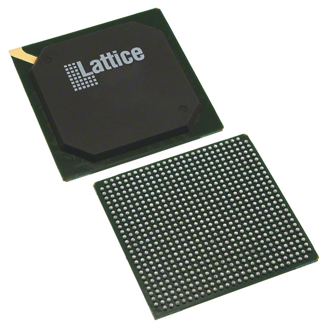
LFE3-150EA-8FN672I

Why Choose Us?
Professional Platform
B2B & B2C purchasingDelivery at full speed
1-2 days deliveryWide variety
Original manufacturers365 days guarantee
Responsible quality
.png)


Tech Specifications
LFE3-150EA-8FN672I Description
Lattice Semiconductor's LFE3-150EA-8FN672I is a field programmable gate array (FPGA) device that belongs to the company's ECP3 series. This device is designed to provide high performance and low power consumption for a wide range of applications.
Description:
The LFE3-150EA-8FN672I is a mid-range FPGA device that features a high-density architecture and a rich set of programmable logic resources. It is available in a compact 672-pin flip-chip ball grid array (FCBGA) package, making it suitable for use in a variety of applications where space is at a premium.
Features:
Some of the key features of the LFE3-150EA-8FN672I include:
- High-performance programmable logic: The device features a high-density architecture with programmable logic blocks, digital signal processing blocks, and memory blocks, making it suitable for a wide range of applications.
- Low power consumption: The LFE3-150EA-8FN672I is designed to operate at low power, making it ideal for battery-powered or energy-sensitive applications.
- High-speed transceivers: The device includes high-speed transceivers that support data rates up to 3.125 Gbps, making it suitable for use in high-speed communication and networking applications.
- Integrated block RAM: The LFE3-150EA-8FN672I includes integrated block RAM, which can be used for data storage and processing.
- Configurable I/O: The device features a wide range of configurable I/O options, making it suitable for use in a variety of applications.
Applications:
The LFE3-150EA-8FN672I is suitable for use in a wide range of applications, including:
- Communications and networking: The high-speed transceivers and configurable I/O options make the LFE3-150EA-8FN672I ideal for use in high-speed communication and networking applications.
- Industrial control: The device's low power consumption and high-performance programmable logic make it suitable for use in industrial control applications.
- Consumer electronics: The compact form factor and low power consumption of the LFE3-150EA-8FN672I make it suitable for use in consumer electronics, such as set-top boxes and gaming consoles.
- Automotive: The device's reliability and low power consumption make it suitable for use in automotive applications, such as infotainment systems and advanced driver assistance systems (ADAS).
- Aerospace and defense: The LFE3-150EA-8FN672I can be used in aerospace and defense applications, such as radar systems and satellite communications.
Overall, the Lattice Semiconductor's LFE3-150EA-8FN672I is a versatile FPGA device that offers high performance, low power consumption, and a wide range of features, making it suitable for use in a variety of applications.
FAQ
Not available to buy online? Want the lower wholesale price? Please Send RFQ to get best price, we will respond immediately


.png?x-oss-process=image/format,webp/resize,h_32)


