
 German
 Japanese
 Portuguese
 Korea
Korea
 Mexico
 Dutch
Dutch


Lattice Semiconductor
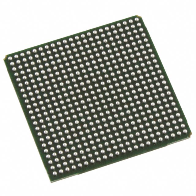
LFE3-70EA-7FN484C

Why Choose Us?
Professional Platform
B2B & B2C purchasingDelivery at full speed
1-2 days deliveryWide variety
Original manufacturers365 days guarantee
Responsible quality
.png)


Tech Specifications
LFE3-70EA-7FN484C Description
Lattice Semiconductor's LFE3-70EA-7FN484C is a field programmable gate array (FPGA) device that offers a range of features and applications for various industries.
Description:
The LFE3-70EA-7FN484C is a low-cost, mid-range FPGA that is designed for a wide range of applications. It is based on Lattice's ECP3 technology, which provides high performance and low power consumption. The device is available in a 484-ball fine pitch ball grid array (FBGA) package, making it suitable for use in a variety of electronic systems.
Features:
Some of the key features of the LFE3-70EA-7FN484C include:
- High performance: The device offers high performance with its 6.6 ns maximum clock speed and 230 MHz maximum operating frequency.
- Low power consumption: The ECP3 technology used in the LFE3-70EA-7FN484C provides low power consumption, making it suitable for battery-powered applications.
- Configurable logic blocks: The device has a flexible architecture with configurable logic blocks (CLBs) that can be used to implement a wide range of digital logic functions.
- Embedded memory: The LFE3-70EA-7FN484C includes embedded memory blocks that can be used for data storage and processing.
- I/O capabilities: The device has a wide range of I/O capabilities, including support for LVDS, serdes, and other high-speed interfaces.
- Security features: The LFE3-70EA-7FN484C includes security features such as encryption and secure boot to protect against unauthorized access and tampering.
Applications:
The LFE3-70EA-7FN484C is suitable for a wide range of applications, including:
- Industrial control systems: The device can be used in industrial control systems for motor control, sensor interfacing, and data processing.
- Communications: The high-speed I/O capabilities of the LFE3-70EA-7FN484C make it suitable for use in communications systems, such as base stations and routers.
- Consumer electronics: The low power consumption and flexible architecture of the device make it suitable for use in consumer electronics, such as smartphones, tablets, and smart home devices.
- Automotive: The LFE3-70EA-7FN484C can be used in automotive applications for infotainment systems, driver assistance systems, and other electronic control units.
- Aerospace and defense: The device can be used in aerospace and defense applications for signal processing, data acquisition, and communication systems.
Overall, the LFE3-70EA-7FN484C is a versatile FPGA device that offers high performance, low power consumption, and a wide range of features suitable for various applications across different industries.
FAQ
Not available to buy online? Want the lower wholesale price? Please Send RFQ to get best price, we will respond immediately


.png?x-oss-process=image/format,webp/resize,h_32)


