
 German
 Japanese
 Portuguese
 Korea
Korea
 Mexico
 Dutch
Dutch


Lattice Semiconductor
LFE5U-85F-7BG381I

Why Choose Us?
Professional Platform
B2B & B2C purchasingDelivery at full speed
1-2 days deliveryWide variety
Original manufacturers365 days guarantee
Responsible quality
.png)


Tech Specifications
LFE5U-85F-7BG381I Description
LFE5U-85F-7BG381I Description
The LFE5U-85F-7BG381I is a high-performance Field Programmable Gate Array (FPGA) from Lattice Semiconductor Corporation, designed to meet the demanding requirements of modern embedded systems. This IC FPGA features a robust architecture with 21,000 Logic Array Blocks (LABs) or Configurable Logic Blocks (CLBs), providing significant computational power and flexibility. It is equipped with 3,833,856 bits of RAM, offering ample storage for complex algorithms and data processing tasks. The device supports a wide range of I/O configurations, with 205 I/O pins, making it highly adaptable for various applications.
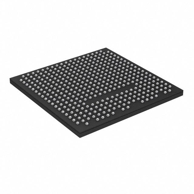
The LFE5U-85F-7BG381I operates within a voltage range of 1.045V to 1.155V, ensuring efficient power usage and compatibility with low-power systems. It is packaged in a 381-ball CABGA (Ceramic Ball Grid Array) format, which is ideal for surface-mount applications and provides excellent thermal performance. The device is RoHS3 compliant and REACH unaffected, ensuring it meets stringent environmental and safety standards. With a moisture sensitivity level (MSL) of 3 (168 hours), it is suitable for use in various environmental conditions.
LFE5U-85F-7BG381I Features
- High Logic Capacity: The LFE5U-85F-7BG381I boasts 84,000 logic elements/cells, providing extensive computational capabilities for complex digital designs.
- Large RAM Capacity: With 3,833,856 RAM bits, this FPGA can handle large datasets and complex algorithms, making it suitable for applications requiring significant memory.
- Flexible I/O Options: The 205 I/O pins offer a wide range of connectivity options, allowing for seamless integration with various peripherals and systems.
- Low Power Operation: Operating within a voltage range of 1.045V to 1.155V, this FPGA is optimized for low power consumption, making it ideal for battery-powered and energy-efficient applications.
- Surface Mount Compatibility: The CABGA package is designed for surface-mount technology, ensuring ease of integration into compact and high-density designs.
- Environmental Compliance: The device is RoHS3 compliant and REACH unaffected, ensuring it meets global environmental and safety regulations.
- Moisture Sensitivity Level: With an MSL of 3 (168 hours), the LFE5U-85F-7BG381I is suitable for a variety of environmental conditions, enhancing its reliability and durability.
LFE5U-85F-7BG381I Applications
The LFE5U-85F-7BG381I is ideal for a range of applications due to its high logic capacity, large RAM, and flexible I/O options. Some specific use cases include:
- Embedded Systems: The high logic capacity and low power operation make it suitable for embedded systems requiring significant processing power and energy efficiency.
- Digital Signal Processing (DSP): The large RAM capacity and flexible I/O options enable efficient implementation of complex DSP algorithms.
- Communication Systems: The extensive I/O capabilities and low power operation make it ideal for communication systems, including base stations and network interfaces.
- Industrial Automation: The robust architecture and environmental compliance make it suitable for industrial applications requiring high reliability and durability.
- Consumer Electronics: The compact CABGA package and low power operation make it ideal for consumer electronics, where space and energy efficiency are critical.
Conclusion of LFE5U-85F-7BG381I
The LFE5U-85F-7BG381I from Lattice Semiconductor is a versatile and high-performance FPGA designed to meet the needs of modern embedded systems. Its extensive logic capacity, large RAM, and flexible I/O options make it suitable for a wide range of applications, from embedded systems to industrial automation. The low power operation and surface-mount compatibility ensure it is ideal for energy-efficient and compact designs. With its environmental compliance and robust architecture, the LFE5U-85F-7BG381I stands out as a reliable and efficient choice for engineers and designers in the electronics industry.
FAQ
| Quantity | Unit Price | Ext. Price |
|---|---|---|
| 1+ | $26.82857 | $26.83 |
| 30+ | $25.47943 | $764.38 |
Not available to buy online? Want the lower wholesale price? Please Send RFQ to get best price, we will respond immediately


.png?x-oss-process=image/format,webp/resize,h_32)


