Lattice Semiconductor
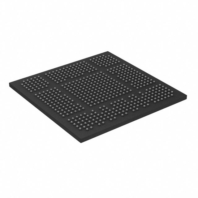
LFE5U-85F-8BG554C
FPGAs


.png?x-oss-process=image/format,webp/resize,p_30)


LFE5U-85F-8BG554C Description
Lattice Semiconductor's LFE5U-85F-8BG554C is a high-performance field-programmable gate array (FPGA) device that offers a wide range of features and applications for various industries.
Description:
The LFE5U-85F-8BG554C is a member of Lattice Semiconductor's low-power, low-cost ECP5 FPGA family. It is based on a fine-grain, low-power architecture that provides high performance and low power consumption. The device features a 28-nm process technology and offers up to 85 K LEs (Look-Up Elements) of programmable logic and up to 2.3 Mbits of memory.
Features:
- Fine-grain, low-power architecture: The LFE5U-85F-8BG554C is designed with a fine-grain, low-power architecture that enables high performance and low power consumption.
- 28-nm process technology: The device is manufactured using a 28-nm process technology, which provides high performance and low power consumption.
- Large programmable logic capacity: The LFE5U-85F-8BG554C offers up to 85 K LEs of programmable logic, providing ample capacity for complex designs.
- High memory capacity: The device features up to 2.3 Mbits of memory, which can be used for data storage and processing.
- Integrated DSP blocks: The LFE5U-85F-8BG554C includes integrated DSP blocks that can be used for high-speed signal processing and data manipulation.
- High-speed I/O: The device supports high-speed I/O interfaces, such as LVDS and DDR, for fast data transfer and communication.
- Security features: The LFE5U-85F-8BG554C includes security features, such as encryption and authentication, to protect sensitive data and intellectual property.
Applications:
The LFE5U-85F-8BG554C is suitable for a wide range of applications, including:
- Industrial control systems: The device's low power consumption and high performance make it ideal for industrial control systems, such as motor control and factory automation.
- Communication systems: The high-speed I/O interfaces and integrated DSP blocks make the LFE5U-85F-8BG554C suitable for communication systems, such as base stations and network infrastructure.
- Consumer electronics: The device's low power consumption and small form factor make it suitable for consumer electronics, such as smartphones, tablets, and wearable devices.
- Automotive systems: The LFE5U-85F-8BG554C can be used in automotive systems, such as infotainment systems, advanced driver assistance systems (ADAS), and powertrain control.
- Security systems: The device's security features make it suitable for security systems, such as surveillance cameras and access control systems.
- Medical devices: The LFE5U-85F-8BG554C can be used in medical devices, such as imaging systems, patient monitoring systems, and diagnostic equipment.
In summary, Lattice Semiconductor's LFE5U-85F-8BG554C is a versatile FPGA device that offers high performance, low power consumption, and a wide range of features suitable for various applications across different industries.
Tech Specifications
LFE5U-85F-8BG554C Documents
Download datasheets and manufacturer documentation for LFE5U-85F-8BG554C
 ECP5, ECP5-5G Family Datasheet
  All Dev Pkg Mark Chg 12/Nov/2018
  Solving Intellegence, Vision, Connectivity Challenges at the Edge with ECP5 FPGAs
  Top Mark Format Change 20/Dec/2023
 Relevant Search
Shopping Guide


.png?x-oss-process=image/format,webp/resize,h_32)


