
Lattice Semiconductor
LFE5UM-25F-7BG381C

Why Choose Us?
Professional Platform
B2B & B2C purchasingDelivery at full speed
1-2 days deliveryWide variety
Original manufacturers365 days guarantee
Responsible quality
.png)


Tech Specifications
LFE5UM-25F-7BG381C Description
Lattice Semiconductor's LFE5UM-25F-7BG381C is a high-performance field-programmable gate array (FPGA) that offers a range of features and applications for various industries.
Description:
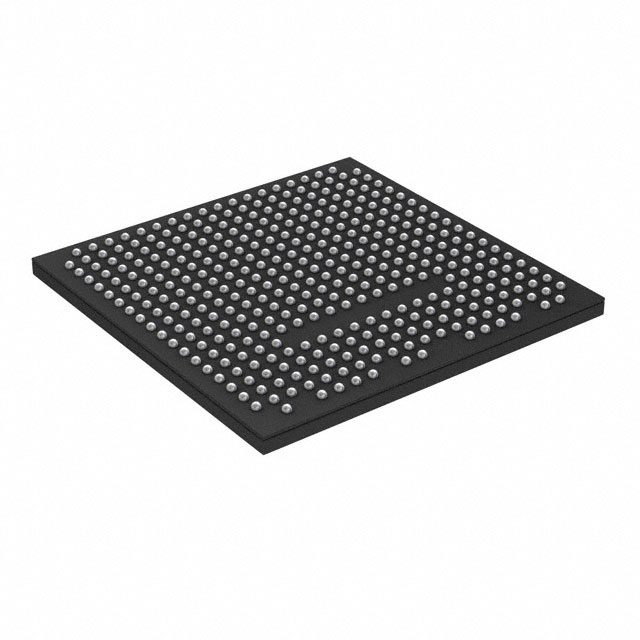
The LFE5UM-25F-7BG381C is a member of Lattice Semiconductor's low-power, mid-range ECP5 FPGA family. This device is designed to provide a balance of power efficiency, performance, and functionality for a wide range of applications. It features a 7x7 mm BGA package, making it suitable for space-constrained designs.
Features:
- Low power consumption: The LFE5UM-25F-7BG381C is designed for energy-efficient operation, making it ideal for battery-powered and portable applications.
- High performance: With a high-speed transceiver and versatile I/O options, this FPGA can handle demanding data processing tasks and communication requirements.
- Versatile I/O options: The device offers a wide range of I/O options, including LVDS, DDR, and high-speed transceivers, allowing it to interface with various peripherals and communication protocols.
- Security features: The LFE5UM-25F-7BG381C includes advanced security features, such as encryption and authentication, to protect sensitive data and intellectual property.
- Flexibility: The mid-range FPGA offers a balance of resources and performance, making it suitable for a wide range of applications, from simple to complex designs.
Applications:
- Industrial automation: The LFE5UM-25F-7BG381C can be used in industrial control systems, providing real-time processing and communication capabilities.
- Communication systems: The FPGA's high-speed transceivers and versatile I/O options make it suitable for communication infrastructure, such as routers, switches, and base stations.
- Automotive: The device can be used in various automotive applications, including infotainment systems, advanced driver assistance systems (ADAS), and in-vehicle networking.
- Consumer electronics: The LFE5UM-25F-7BG381C can be used in portable devices, such as smartphones, tablets, and wearables, for processing and communication tasks.
- Aerospace and defense: The FPGA's security features and high reliability make it suitable for aerospace and defense applications, such as navigation systems, communication equipment, and electronic warfare systems.
In summary, Lattice Semiconductor's LFE5UM-25F-7BG381C is a versatile, low-power FPGA that offers a range of features and applications for various industries. Its balance of power efficiency, performance, and functionality make it an ideal choice for demanding applications in industrial automation, communication systems, automotive, consumer electronics, and aerospace and defense.
FAQ
Not available to buy online? Want the lower wholesale price? Please Send RFQ to get best price, we will respond immediately


.png?x-oss-process=image/format,webp/resize,h_32)


