
 German
 Japanese
 Portuguese
 Korea
Korea
 Mexico
 Dutch
Dutch


Lattice Semiconductor
LFXP2-5E-6MN132C

Why Choose Us?
Professional Platform
B2B & B2C purchasingDelivery at full speed
1-2 days deliveryWide variety
Original manufacturers365 days guarantee
Responsible quality
.png)


Tech Specifications
LFXP2-5E-6MN132C Description
Lattice Semiconductor's LFXP2-5E-6MN132C is a high-performance programmable logic device designed for a wide range of applications. This device is part of the LatticeECP2 family, which offers a combination of low power consumption, high performance, and small form factor.
Description:
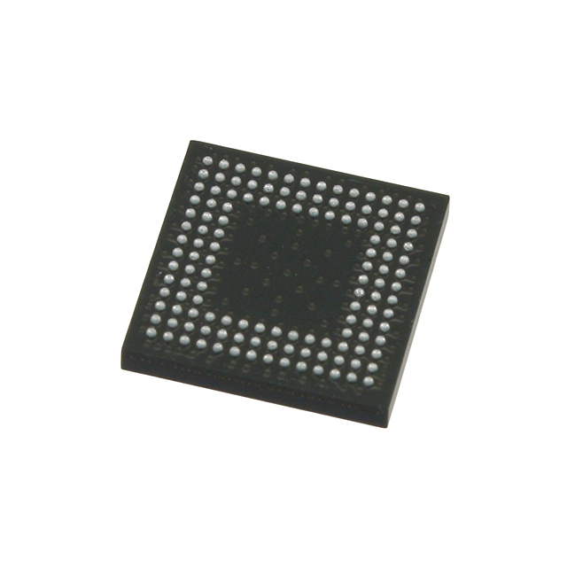
The LFXP2-5E-6MN132C is a programmable logic device that features a 5.0 V core voltage and a 3.3 V I/O voltage. It has a programmable logic array with 6,000 logic elements and 132 I/O pins, making it suitable for complex and high-density designs. The device is available in a plastic ball grid array (PBGA) package, which is compact and suitable for various applications.
Features:
- Low power consumption: The LFXP2-5E-6MN132C is designed for low power applications, making it ideal for battery-powered devices or systems with power constraints.
- High performance: The device offers high-speed operation and a large number of logic elements, allowing for the implementation of complex designs.
- Versatile I/O options: With 132 I/O pins, the LFXP2-5E-6MN132C can support a wide range of input/output requirements.
- Small form factor: The PBGA package is compact, making it suitable for applications where space is limited.
- Programmable logic: The device can be programmed to implement custom logic functions, providing flexibility and adaptability for various applications.
Applications:
The LFXP2-5E-6MN132C is suitable for a wide range of applications, including but not limited to:
- Industrial control systems: The device's low power consumption and high performance make it ideal for industrial control applications, such as motor control, sensor interfacing, and data acquisition systems.
- Communication systems: The LFXP2-5E-6MN132C can be used in communication systems, such as transceivers, modems, and network infrastructure equipment.
- Consumer electronics: The small form factor and versatile I/O options make the device suitable for consumer electronics, such as smartphones, tablets, and wearable devices.
- Automotive systems: The LFXP2-5E-6MN132C can be used in automotive applications, such as infotainment systems, advanced driver assistance systems (ADAS), and power management systems.
- Medical devices: The device's low power consumption and high performance make it suitable for medical devices, such as imaging systems, patient monitoring equipment, and diagnostic devices.
In summary, Lattice Semiconductor's LFXP2-5E-6MN132C is a high-performance, low power, and versatile programmable logic device that is suitable for a wide range of applications, from industrial control systems to consumer electronics and medical devices. Its small form factor, large number of I/O pins, and programmable logic make it an ideal choice for designers looking for flexibility and adaptability in their projects.
FAQ
Not available to buy online? Want the lower wholesale price? Please Send RFQ to get best price, we will respond immediately


.png?x-oss-process=image/format,webp/resize,h_32)


