
 German
 Japanese
 Portuguese
 Korea
Korea
 Mexico
 Dutch
Dutch


Lattice Semiconductor
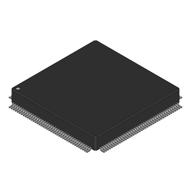
OR2C08A4J160-DB

Why Choose Us?
Professional Platform
B2B & B2C purchasingDelivery at full speed
1-2 days deliveryWide variety
Original manufacturers365 days guarantee
Responsible quality
.png)


Tech Specifications
OR2C08A4J160-DB Description
The Lattice Semiconductor OR2C08A4J160-DB is a high-performance programmable logic device that is designed to meet the needs of a wide range of applications. This device is part of Lattice's OR2C family of FPGAs (Field Programmable Gate Arrays), which are known for their low power consumption, small form factor, and high performance.
Description:
The OR2C08A4J160-DB is a compact and versatile FPGA that offers a range of features and capabilities. It is based on Lattice's advanced low-power 28 nm process technology, which enables it to deliver high performance while consuming minimal power. The device is available in a compact 256-ball fine-pitch ball grid array (FBGA) package, making it suitable for use in a wide range of applications where space is at a premium.
Features:
Some of the key features of the OR2C08A4J160-DB include:
- Low power consumption: The OR2C08A4J160-DB is designed to operate at low voltages and with low power consumption, making it ideal for use in battery-powered devices or other applications where power efficiency is critical.
- High performance: The device offers high-speed performance and a range of features that make it suitable for a wide range of applications, including communications, industrial control, and consumer electronics.
- Flexibility: The OR2C08A4J160-DB is a highly flexible device that can be programmed to perform a wide range of functions. This makes it suitable for use in a wide range of applications, from simple I/O expansion to complex digital signal processing.
- Small form factor: The compact size of the OR2C08A4J160-DB makes it suitable for use in a wide range of applications where space is limited.
Applications:
The OR2C08A4J160-DB is suitable for a wide range of applications, including:
- Communications: The device can be used in a variety of communication systems, including wireless base stations, routers, and switches.
- Industrial control: The OR2C08A4J160-DB can be used in industrial control systems to provide flexible and programmable control solutions.
- Consumer electronics: The device can be used in a wide range of consumer electronics applications, including set-top boxes, gaming consoles, and smart home devices.
- Automotive: The OR2C08A4J160-DB can be used in automotive applications, such as infotainment systems and advanced driver assistance systems (ADAS).
- IoT: The device can be used in Internet of Things (IoT) applications, where low power consumption and small form factor are critical.
In summary, the Lattice Semiconductor OR2C08A4J160-DB is a high-performance, low-power FPGA that offers a range of features and capabilities. Its compact size and flexibility make it suitable for use in a wide range of applications, from communications to consumer electronics and beyond.
FAQ
Not available to buy online? Want the lower wholesale price? Please Send RFQ to get best price, we will respond immediately


.png?x-oss-process=image/format,webp/resize,h_32)


