
 German
 Japanese
 Portuguese
 Korea
Korea
 Mexico
 Dutch
Dutch


Microchip Technology
A2F500M3G-FGG256I

Why Choose Us?
Professional Platform
B2B & B2C purchasingDelivery at full speed
1-2 days deliveryWide variety
Original manufacturers365 days guarantee
Responsible quality
.png)


Tech Specifications
A2F500M3G-FGG256I Description
A2F500M3G-FGG256I Description
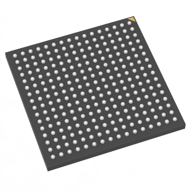
The A2F500M3G-FGG256I is a high-performance, versatile embedded IC chip developed by Microchip Technology, designed for a wide range of applications requiring robust processing capabilities and extensive connectivity options. This product is part of the SmartFusion® series, known for its advanced integration of microcontroller (MCU) and field-programmable gate array (FPGA) functionalities. The A2F500M3G-FGG256I operates at a speed of 80MHz, providing efficient performance for complex tasks. It features a Cortex-M3 processor core, ensuring high-speed processing and low power consumption. The device is housed in a 256-pin BGA package, making it suitable for compact and high-density designs.
A2F500M3G-FGG256I Features
- Speed: The A2F500M3G-FGG256I operates at a frequency of 80MHz, offering fast processing capabilities that are essential for real-time applications.
- Architecture: This device combines the flexibility of an FPGA with the ease of use of an MCU, providing a powerful platform for both hardware and software development.
- Memory: Equipped with 512KB of flash memory and 64KB of RAM, the A2F500M3G-FGG256I can handle large datasets and complex algorithms, making it ideal for embedded systems requiring substantial storage and processing power.
- Peripherals: The A2F500M3G-FGG256I includes a variety of peripherals such as DMA, POR, and WDT, which enhance its functionality and reliability.
- Connectivity: This IC chip supports multiple connectivity options, including EBI/EMI, Ethernet, I2C, SPI, and UART/USART, making it highly adaptable for various communication needs.
- Compliance: The A2F500M3G-FGG256I is REACH unaffected and RoHS3 compliant, ensuring it meets the highest environmental and safety standards.
- Packaging: The device is available in a tray package, which is suitable for automated assembly processes and ensures high reliability in manufacturing.
- Moisture Sensitivity Level (MSL): With an MSL of 3 (168 hours), the A2F500M3G-FGG256I is designed to withstand moisture exposure during manufacturing processes, reducing the risk of damage.
A2F500M3G-FGG256I Applications
The A2F500M3G-FGG256I is ideal for a variety of applications due to its powerful processing capabilities and extensive connectivity options. Some specific use cases include:
- Industrial Automation: The combination of MCU and FPGA functionalities makes it suitable for controlling complex machinery and systems, where real-time processing and hardware customization are required.
- Telecommunications: The Ethernet connectivity and high-speed processing capabilities make it ideal for network infrastructure applications, such as routers and switches.
- Medical Devices: The device's reliability and compliance with environmental standards make it suitable for medical equipment, where precision and safety are paramount.
- Automotive Systems: The A2F500M3G-FGG256I can be used in advanced driver-assistance systems (ADAS) and other automotive applications requiring high performance and low power consumption.
Conclusion of A2F500M3G-FGG256I
The A2F500M3G-FGG256I is a versatile and powerful embedded IC chip that offers a unique blend of MCU and FPGA functionalities. Its high-speed processing capabilities, extensive memory, and diverse connectivity options make it suitable for a wide range of applications. The device's compliance with environmental and safety standards ensures it meets the requirements of modern electronics manufacturing. Whether used in industrial automation, telecommunications, medical devices, or automotive systems, the A2F500M3G-FGG256I provides a reliable and efficient solution for complex embedded systems.
FAQ
Not available to buy online? Want the lower wholesale price? Please Send RFQ to get best price, we will respond immediately


.png?x-oss-process=image/format,webp/resize,h_32)


