
 German
 Japanese
 Portuguese
 Korea
Korea
 Mexico
 Dutch
Dutch


Microchip Technology
AT49BV040B-TU

Why Choose Us?
Professional Platform
B2B & B2C purchasingDelivery at full speed
1-2 days deliveryWide variety
Original manufacturers365 days guarantee
Responsible quality
.png)


Tech Specifications
AT49BV040B-TU Description
AT49BV040B-TU Description
The AT49BV040B-TU is a 4 Mbit (512K x 8) Flash memory IC chip designed for high-performance applications requiring reliable and efficient data storage. Manufactured by Microchip Technology, this chip features a parallel memory interface, making it suitable for systems that demand fast data access and transfer rates. The AT49BV040B-TU operates within a wide voltage range of 2.7V to 3.6V and 4.5V to 5.5V, ensuring compatibility with various power supply configurations.
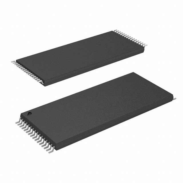
This Flash memory chip is housed in a 32TSOP package, which is ideal for surface-mount applications, providing a compact and robust solution for modern electronic designs. The AT49BV040B-TU boasts an access time of 70 ns and a write cycle time of 120µs for word and page operations, ensuring rapid data read and write capabilities. Despite being marked as obsolete, the AT49BV040B-TU remains a valuable component for legacy systems and applications where its specific features are still required.
AT49BV040B-TU Features
- Memory Organization: The AT49BV040B-TU is organized as 512K x 8, offering a total memory capacity of 4 Mbit. This configuration allows for efficient storage and retrieval of data in systems that require moderate to high memory density.
- Parallel Interface: The parallel memory interface ensures fast data transfer rates, making it suitable for applications that demand high-speed data processing.
- Wide Operating Voltage Range: The chip operates within a wide voltage range of 2.7V to 3.6V and 4.5V to 5.5V, providing flexibility in power supply design and ensuring compatibility with various electronic systems.
- Fast Access and Write Times: With an access time of 70 ns and a write cycle time of 120µs, the AT49BV040B-TU delivers rapid data read and write capabilities, enhancing overall system performance.
- Surface-Mount Compatibility: The 32TSOP package is designed for surface-mount technology (SMT), ensuring a compact and reliable solution for modern PCB designs.
- Moisture Sensitivity Level: The AT49BV040B-TU has a moisture sensitivity level (MSL) of 3 (168 hours), making it suitable for manufacturing processes that require protection against moisture exposure.
- Compliance: The chip is REACH unaffected and RoHS3 compliant, ensuring it meets environmental and regulatory standards for electronic components.
AT49BV040B-TU Applications
The AT49BV040B-TU is ideal for a variety of applications where reliable and efficient data storage is required. Some specific use cases include:
- Embedded Systems: The chip's fast access and write times make it suitable for embedded systems that require rapid data processing and storage.
- Industrial Control Systems: The wide operating voltage range and robust surface-mount package make the AT49BV040B-TU ideal for industrial applications where reliability and durability are critical.
- Telecommunications: The parallel interface and fast data transfer capabilities are beneficial for telecommunications equipment that requires high-speed data storage and retrieval.
- Consumer Electronics: The compact 32TSOP package and surface-mount compatibility make the AT49BV040B-TU suitable for consumer electronics where space is a constraint.
Conclusion of AT49BV040B-TU
The AT49BV040B-TU is a versatile and reliable Flash memory IC chip that offers a balance of performance and compatibility. Its fast access and write times, wide operating voltage range, and robust surface-mount package make it an ideal solution for a variety of applications, from embedded systems to industrial control and telecommunications. Despite being marked as obsolete, the AT49BV040B-TU remains a valuable component for legacy systems and applications where its specific features are still required. Its compliance with environmental and regulatory standards ensures it meets the requirements of modern electronic design and manufacturing processes.
FAQ
Not available to buy online? Want the lower wholesale price? Please Send RFQ to get best price, we will respond immediately


.png?x-oss-process=image/format,webp/resize,h_32)


