
 German
 Japanese
 Portuguese
 Korea
Korea
 Mexico
 Dutch
Dutch


Microchip Technology
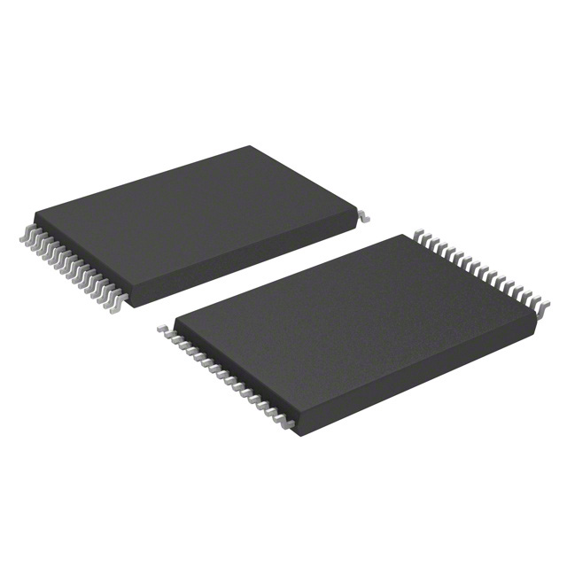
AT49F002ANT-55VU

Why Choose Us?
Professional Platform
B2B & B2C purchasingDelivery at full speed
1-2 days deliveryWide variety
Original manufacturers365 days guarantee
Responsible quality
.png)


Tech Specifications
AT49F002ANT-55VU Description
AT49F002ANT-55VU Description
The AT49F002ANT-55VU is a high-performance 2Mbit Flash memory IC designed for a wide range of embedded applications. Manufactured by Microchip Technology, this device features a parallel memory interface and is organized as 256K x 8 bits. It is housed in a 32VSOP package, making it suitable for surface-mount applications. The AT49F002ANT-55VU operates within a voltage range of 4.5V to 5.5V and offers an access time of 55 nanoseconds, ensuring fast data retrieval. With a write cycle time of 50 microseconds, it provides efficient data storage and retrieval capabilities. This Flash memory IC is REACH unaffected and RoHS3 compliant, adhering to stringent environmental and safety standards. The product is categorized under Memory IC Chips and is identified by the base product number AT49F002. Although it is now obsolete, the AT49F002ANT-55VU remains a reliable choice for legacy systems and specific applications where its unique features are required.
AT49F002ANT-55VU Features
- Memory Organization: The AT49F002ANT-55VU is organized as 256K x 8 bits, providing a total memory size of 2Mbit. This configuration is ideal for applications requiring a moderate amount of non-volatile storage.
- Parallel Interface: The parallel memory interface ensures high-speed data transfer, making it suitable for applications where rapid data access is critical.
- Fast Access Time: With an access time of 55 nanoseconds, the AT49F002ANT-55VU delivers quick data retrieval, enhancing overall system performance.
- Efficient Write Cycle: The write cycle time of 50 microseconds allows for efficient data storage, ensuring that data can be written and read back quickly.
- Wide Voltage Range: The device operates within a voltage range of 4.5V to 5.5V, providing flexibility in power supply requirements.
- Surface-Mount Packaging: The 32VSOP package is designed for surface-mount technology, making it suitable for compact and high-density PCB designs.
- Environmental Compliance: The AT49F002ANT-55VU is REACH unaffected and RoHS3 compliant, ensuring it meets environmental and safety standards.
- Moisture Sensitivity Level: With an MSL rating of 3 (168 hours), the device is suitable for standard manufacturing processes without requiring special handling for moisture sensitivity.
AT49F002ANT-55VU Applications
The AT49F002ANT-55VU is well-suited for a variety of applications where reliable and efficient non-volatile memory is required. Some specific use cases include:
- Embedded Systems: Ideal for embedded systems that require fast data access and moderate storage capacity. The parallel interface and fast access time ensure smooth operation in real-time applications.
- Industrial Control: Suitable for industrial control systems where data integrity and quick response times are crucial. The wide voltage range and surface-mount packaging make it adaptable to various industrial environments.
- Telecommunications: Can be used in telecommunications equipment for storing firmware and configuration data. The Flash memory format ensures data retention even in the absence of power.
- Consumer Electronics: Applicable in consumer electronics for storing boot code and other critical data. The compact 32VSOP package allows for integration into space-constrained designs.
Conclusion of AT49F002ANT-55VU
The AT49F002ANT-55VU is a robust and reliable 2Mbit Flash memory IC designed for applications requiring fast data access and moderate storage capacity. Its parallel memory interface, fast access time, and efficient write cycle time make it an excellent choice for embedded systems, industrial control, telecommunications, and consumer electronics. Despite being obsolete, the AT49F002ANT-55VU remains a viable option for legacy systems and specific applications where its unique features are essential. Its compliance with environmental and safety standards ensures it meets modern manufacturing requirements.
FAQ
Not available to buy online? Want the lower wholesale price? Please Send RFQ to get best price, we will respond immediately


.png?x-oss-process=image/format,webp/resize,h_32)


