
 German
 Japanese
 Portuguese
 Korea
Korea
 Mexico
 Dutch
Dutch


Microchip Technology
AT49F040-70JC

Why Choose Us?
Professional Platform
B2B & B2C purchasingDelivery at full speed
1-2 days deliveryWide variety
Original manufacturers365 days guarantee
Responsible quality
.png)


Tech Specifications
AT49F040-70JC Description
AT49F040-70JC Description
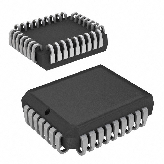
The AT49F040-70JC is a 4 Mbit Flash memory IC chip designed by Microchip Technology. This device is organized as 512K x 8, offering a parallel memory interface for efficient data transfer. It operates within a supply voltage range of 4.5V to 5.5V and is capable of functioning in an ambient temperature range of 0°C to 70°C. The AT49F040-70JC is housed in a surface-mount package and is available in a tube format, making it suitable for automated assembly processes. This Flash memory chip has an access time of 70 ns and a write cycle time of 50µs for word and page operations. Despite its obsolete status, the AT49F040-70JC remains a reliable choice for applications requiring non-volatile memory storage. It is classified under HTSUS code 8542.32.0071 and is REACH unaffected, ensuring compliance with environmental regulations.
AT49F040-70JC Features
- Memory Size and Organization: The AT49F040-70JC offers a 4 Mbit memory size, organized as 512K x 8, providing ample storage for various applications.
- Parallel Interface: The parallel memory interface ensures fast and efficient data transfer, making it suitable for high-speed applications.
- Fast Access and Write Times: With an access time of 70 ns and a write cycle time of 50µs, the AT49F040-70JC delivers rapid data read and write capabilities.
- Wide Operating Voltage Range: The device operates within a supply voltage range of 4.5V to 5.5V, offering flexibility in power supply requirements.
- Temperature Range: The AT49F040-70JC is designed to function reliably within an ambient temperature range of 0°C to 70°C, making it suitable for a variety of environmental conditions.
- Surface-Mount Packaging: The surface-mount package and tube format facilitate easy integration into modern PCB designs and support automated assembly processes.
- Compliance and Safety: The AT49F040-70JC is REACH unaffected and classified under HTSUS code 8542.32.0071, ensuring compliance with environmental and safety regulations.
AT49F040-70JC Applications
The AT49F040-70JC is ideal for a range of applications requiring non-volatile memory storage. Its fast access and write times, combined with a parallel memory interface, make it suitable for high-speed data processing and storage tasks. Some specific use cases include:
- Embedded Systems: The AT49F040-70JC can be used in embedded systems where reliable and fast non-volatile memory is required for firmware storage and data logging.
- Industrial Control: In industrial applications, the device can store critical control parameters and operational data, ensuring system reliability and performance.
- Telecommunications: The AT49F040-70JC can be employed in telecommunication equipment for storing configuration data and firmware, supporting efficient system operation and maintenance.
- Consumer Electronics: The device can be used in consumer electronics for storing user settings, firmware updates, and other non-volatile data, enhancing product functionality and user experience.
Conclusion of AT49F040-70JC
The AT49F040-70JC is a robust and reliable 4 Mbit Flash memory IC chip designed for a variety of applications requiring non-volatile memory storage. Its fast access and write times, combined with a parallel memory interface and wide operating voltage range, make it an excellent choice for high-speed data processing and storage tasks. Despite its obsolete status, the AT49F040-70JC remains a viable option for applications where its unique features and performance benefits are required. Its compliance with environmental and safety regulations ensures that it meets industry standards for responsible manufacturing and usage.
FAQ
Not available to buy online? Want the lower wholesale price? Please Send RFQ to get best price, we will respond immediately


.png?x-oss-process=image/format,webp/resize,h_32)


