
Microchip Technology
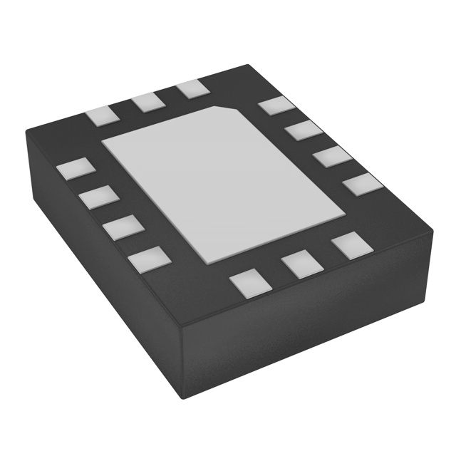
DSA557-0333FL1TVAO
Application Specific Clock/Timing ICs


.png?x-oss-process=image/format,webp/resize,p_30)


DSA557-0333FL1TVAO Description
DSA557-0333FL1TVAO Description
The DSA557-0333FL1TVAO is a high-performance, 2-output auto-grade MEMS clock generator specifically designed for PCI Express (PCIe) applications. Manufactured by Microchip Technology, this device is optimized for reliability and performance in demanding environments. The DSA557-0333FL1TVAO features a 1:2 input-to-output ratio, supporting differential input and single-ended output, making it highly versatile for various clocking needs. With a maximum operating frequency of 100MHz, it is well-suited for high-speed data transfer applications. The device supports multiple output formats, including HCSL, LVCMOS, and LVDS, providing flexibility in system design. The inclusion of a Phase-Locked Loop (PLL) ensures precise frequency control and stability. The DSA557-0333FL1TVAO operates within a supply voltage range of 2.25V to 3.63V, making it compatible with a wide range of power supply configurations. It is packaged in a surface-mount Tape & Reel (TR) format, facilitating easy integration into modern PCB designs. The device is REACH unaffected and ROHS3 compliant, ensuring environmental sustainability and regulatory compliance. With a moisture sensitivity level (MSL) of 1 (unlimited), it is highly resistant to environmental moisture, enhancing its durability and reliability.
DSA557-0333FL1TVAO Features
- High-Speed Performance: Capable of operating up to 100MHz, the DSA557-0333FL1TVAO is ideal for high-speed data transfer applications, ensuring minimal latency and maximum throughput.
- Versatile Output Options: Supports HCSL, LVCMOS, and LVDS output formats, providing design engineers with the flexibility to choose the most suitable output type for their specific application requirements.
- Differential Input and Single-Ended Output: The device features differential input and single-ended output capabilities, enhancing signal integrity and reducing electromagnetic interference (EMI).
- Phase-Locked Loop (PLL): The integrated PLL ensures precise frequency control and stability, making the DSA557-0333FL1TVAO highly reliable for critical clocking applications.
- Wide Supply Voltage Range: Operates within a supply voltage range of 2.25V to 3.63V, offering compatibility with various power supply configurations and reducing the need for additional voltage regulation components.
- Surface-Mount Packaging: The surface-mount Tape & Reel (TR) packaging format facilitates easy integration into modern PCB designs, enhancing manufacturing efficiency and reducing assembly costs.
- Environmental Compliance: REACH unaffected and ROHS3 compliant, ensuring environmental sustainability and regulatory compliance, making it suitable for global markets.
- Moisture Resistance: With a moisture sensitivity level (MSL) of 1 (unlimited), the DSA557-0333FL1TVAO is highly resistant to environmental moisture, enhancing its durability and reliability in various operating conditions.
DSA557-0333FL1TVAO Applications
The DSA557-0333FL1TVAO is ideal for a wide range of applications, particularly those requiring high-speed clocking and reliable performance. Key applications include:
- PCI Express (PCIe) Systems: The device's high-speed performance and differential input capabilities make it well-suited for PCIe applications, ensuring reliable clocking and minimal latency.
- High-Speed Data Transfer: Its ability to operate up to 100MHz makes it ideal for applications requiring high-speed data transfer, such as networking equipment, storage devices, and high-performance computing systems.
- Automotive Electronics: The auto-grade design and high reliability make the DSA557-0333FL1TVAO suitable for automotive applications, where robustness and performance are critical.
- Industrial Control Systems: The device's wide supply voltage range and environmental compliance make it suitable for industrial control systems, where reliability and durability are paramount.
- Telecommunications: The DSA557-0333FL1TVAO's versatile output options and high-speed performance make it ideal for telecommunications applications, ensuring precise clocking and minimal signal degradation.
Conclusion of DSA557-0333FL1TVAO
The DSA557-0333FL1TVAO is a highly reliable and versatile MEMS clock generator designed for PCI Express (PCIe) applications. Its high-speed performance, versatile output options, and integrated PLL make it an ideal choice for applications requiring precise clocking and high reliability. The wide supply voltage range, surface-mount packaging, and environmental compliance further enhance its suitability for a variety of industries. Whether used in high-speed data transfer systems, automotive electronics, or industrial control systems, the DSA557-0333FL1TVAO offers exceptional performance and reliability, making it a standout choice in the clocking IC market.
Tech Specifications
DSA557-0333FL1TVAO Documents
Download datasheets and manufacturer documentation for DSA557-0333FL1TVAO
 DSA557-03/04/05
  DSA557-03/04/05
  DSA557-03/04/05 Datasheet 31/Jul/2023
  Microchip CA Prop65 Microchip RoHS Microchip REACH
 Shopping Guide


.png?x-oss-process=image/format,webp/resize,h_32)


