
Microchip Technology
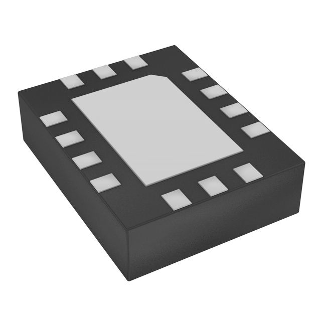
DSC557-0333FI1T
Application Specific Clock/Timing ICs


.png?x-oss-process=image/format,webp/resize,p_30)


DSC557-0333FI1T Description
DSC557-0333FI1T Description
The DSC557-0333FI1T is a high-performance, 2-output MEMS clock generator specifically designed for PCI Express (PCIe) Gen1/2/3/4 applications. Manufactured by Microchip Technology, this device offers a robust and reliable solution for generating precise timing signals in various electronic systems. The DSC557-0333FI1T features a wide operating voltage range of 2.25V to 3.6V and supports multiple output formats, including HCSL, LVCMOS, and LVDS, making it highly versatile for different application requirements.
DSC557-0333FI1T Features
- Main Purpose: The primary application of the DSC557-0333FI1T is to provide clock signals for PCI Express (PCIe) Gen1/2/3/4 interfaces, ensuring accurate and reliable timing for high-speed data transfers.
- PLL Integration: Equipped with a Phase-Locked Loop (PLL), the DSC557-0333FI11T can generate stable and precise clock signals, maintaining synchronization with the input reference clock.
- Output Options: The device supports multiple output formats, including HCSL, LVCMOS, and LVDS, providing flexibility to match various system requirements.
- Frequency Range: With a maximum output frequency of 100MHz, the DSC557-0333FI1T is suitable for a wide range of applications requiring high-speed clocking.
- Differential Signaling: The DSC557-0333FI1T supports differential signaling (LVDS) for the output, which helps in reducing electromagnetic interference (EMI) and improving signal integrity over long distances.
- Mounting Type: Surface mount technology (SMT) allows for efficient and compact integration into modern PCB designs.
- Compliance and Standards: The DSC557-0333FI1T is REACH unaffected and RoHS3 compliant, ensuring it meets environmental and safety standards.
- Packaging: Available in a Tape & Reel (TR) package, the DSC557-0333FI1T is suitable for automated assembly processes, enhancing manufacturing efficiency.
DSC557-0333FI1T Applications
The DSC557-0333FI1T is ideal for applications requiring precise clock generation and synchronization, particularly in high-speed data transfer systems. Some specific use cases include:
- PCI Express Systems: The DSC557-0333FI1T is specifically designed for PCIe Gen1/2/3/4 applications, providing accurate clock signals to ensure reliable data transfer and communication.
- Data Centers: In data centers, the DSC557-0333FI1T can be used to synchronize clock signals across multiple servers and storage devices, ensuring efficient data processing and transfer.
- Networking Equipment: Routers, switches, and other networking devices can benefit from the precise timing provided by the DSC557-0333FI1T, ensuring reliable and high-speed data communication.
- Consumer Electronics: High-speed interfaces in consumer electronics, such as graphics cards and SSDs, can utilize the DSC557-0333FI1T to maintain accurate clocking and improve overall system performance.
Conclusion of DSC557-0333FI1T
The DSC557-0333FI1T is a versatile and high-performance MEMS clock generator designed for PCI Express applications. Its wide operating voltage range, multiple output formats, and support for differential signaling make it a reliable choice for various high-speed data transfer systems. The integration of a PLL ensures stable and precise clock generation, while its compliance with environmental and safety standards makes it suitable for modern electronic designs. Whether in data centers, networking equipment, or consumer electronics, the DSC557-0333FI1T offers a robust solution for accurate clocking and synchronization.
Tech Specifications
DSC557-0333FI1T Documents
Download datasheets and manufacturer documentation for DSC557-0333FI1T
 DSC557-03
  Marking Change 17/Nov/2020 DSC557-03-04-05 31/Mar/2023
  Microchip CA Prop65 Microchip RoHS Microchip REACH
 Shopping Guide


.png?x-oss-process=image/format,webp/resize,h_32)


