
 German
 Japanese
 Portuguese
 Korea
Korea
 Mexico
 Dutch
Dutch


Microchip Technology
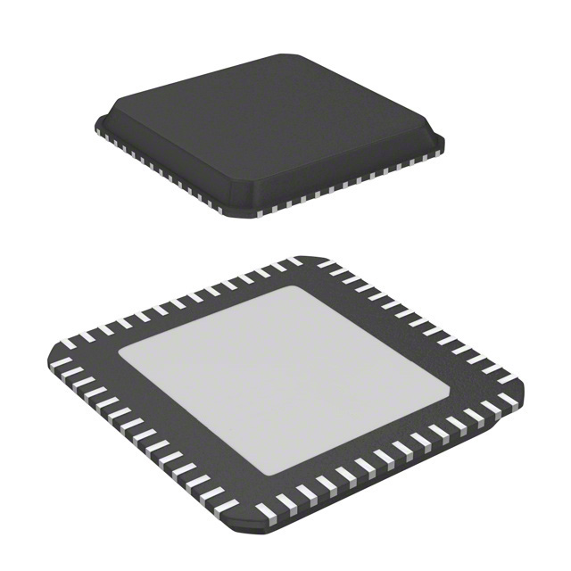
HV2809K6-G

Why Choose Us?
Professional Platform
B2B & B2C purchasingDelivery at full speed
1-2 days deliveryWide variety
Original manufacturers365 days guarantee
Responsible quality
.png)


Tech Specifications
HV2809K6-G Description
HV2809K6-G Description
The HV2809K6-G is a high-performance, 2:1 multiplexer/demultiplexer IC designed for demanding applications such as ultrasound imaging. Manufactured by Microchip Technology, this interface IC chip is part of the HV2809 family and is optimized for high reliability and efficiency in a compact 56VFQFN package. The device operates within a temperature range of 0°C to 70°C (TA) and supports a wide supply voltage range, making it suitable for various power configurations.
HV2809K6-G Features
- Wide Operating Temperature Range: The HV2809K6-G operates reliably within a temperature range of 0°C to 70°C (TA), ensuring stable performance in diverse environmental conditions.
- Broad Voltage Compatibility: This IC supports dual supply voltages from ±40V to ±160V and single supply voltages from 40V to 200V, providing flexibility in power supply design.
- High Bandwidth: With a -3dB bandwidth of 50MHz, the HV2809K6-G ensures minimal signal degradation and high fidelity in high-frequency applications.
- Low On-State Resistance: The maximum on-state resistance of 38Ω minimizes power loss and improves overall system efficiency.
- Surface Mount Packaging: The surface mount type (SMT) packaging facilitates easy integration into modern PCB designs, enhancing reliability and reducing assembly time.
- Compliance and Safety: The HV2809K6-G is REACH unaffected and RoHS3 compliant, meeting stringent environmental and safety standards.
- Moisture Sensitivity Level: With an MSL rating of 3 (168 hours), the device is well-suited for environments with varying humidity levels.
- Multiplexer/Demultiplexer Circuit: The 2:1 multiplexer/demultiplexer circuit design allows for efficient signal routing and switching, ideal for applications requiring signal multiplexing.
HV2809K6-G Applications
The HV2809K6-G is particularly well-suited for applications in the medical imaging sector, specifically ultrasound systems. Its high bandwidth and low on-state resistance ensure clear and accurate imaging, while its wide voltage range and robust packaging make it reliable in demanding medical environments. The device's ability to handle high-frequency signals without degradation makes it an ideal choice for systems requiring precise signal processing.
Conclusion of HV2809K6-G
The HV2809K6-G from Microchip Technology is a versatile and reliable high-voltage multiplexer/demultiplexer IC. Its wide operating temperature range, broad voltage compatibility, and high bandwidth make it an excellent choice for high-performance applications such as ultrasound imaging. The low on-state resistance and surface mount packaging further enhance its efficiency and ease of integration. With compliance to REACH and RoHS3 standards, the HV2809K6-G not only meets technical requirements but also adheres to environmental and safety regulations. This IC is a standout solution for engineers seeking a robust and efficient signal routing component for their high-frequency applications.
FAQ
| Quantity | Unit Price | Ext. Price |
|---|---|---|
| 1+ | $20.78560 | $20.79 |
| 25+ | $17.31840 | $432.96 |
| 100+ | $15.73440 | $1573.44 |
Not available to buy online? Want the lower wholesale price? Please Send RFQ to get best price, we will respond immediately


.png?x-oss-process=image/format,webp/resize,h_32)


