
Microchip Technology
HV9150K6-G
DC DC Switching Controllers


.png?x-oss-process=image/format,webp/resize,p_30)


HV9150K6-G Description
HV9150K6-G Description
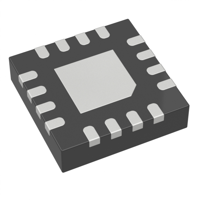
The HV9150K6-G is a high-performance DC-DC switching controller designed by Microchip Technology, specifically tailored for boost topology applications. This transistor driver features a positive output configuration and is optimized for switching frequencies ranging from 40kHz to 400kHz, making it highly versatile for various power conversion needs. The device operates within a supply voltage range of 2.7V to 4.5V, ensuring compatibility with a wide array of power supply systems. Its active product status and compliance with REACH and ROHS3 standards highlight its reliability and suitability for modern electronics manufacturing.
HV9150K6-G Features
- Output Type: Transistor Driver
- Output Configuration: Positive
- Frequency - Switching: 40kHz to 400kHz
- Voltage - Supply (Vcc/Vdd): 2.7V to 4.5V
- Control Features: Enable, Frequency Control
- Duty Cycle (Max): 87.5%
- Output Phases: 1
- Number of Outputs: 1
- Mounting Type: Surface Mount
- Moisture Sensitivity Level (MSL): 3 (168 Hours)
- Synchronous Rectifier: No
- Clock Sync: No
- Package: Tape & Reel (TR)
- HTSUS: 8542.39.0001
- ECCN: EAR99
The HV9150K6-G offers several unique features that set it apart from similar models. Its wide switching frequency range allows for flexibility in design, enabling engineers to optimize for efficiency and performance across various operating conditions. The device's control features, including enable and frequency control, provide precise control over the switching process, enhancing overall system reliability and efficiency. Additionally, its surface mount packaging and moisture sensitivity level of 3 (168 Hours) make it well-suited for high-volume manufacturing processes and applications requiring robust environmental protection.
HV9150K6-G Applications
The HV9150K6-G is ideal for a variety of applications where efficient power conversion and reliable performance are critical. Its boost topology makes it particularly well-suited for applications such as LED lighting, where it can efficiently drive high-brightness LEDs with minimal power loss. The device is also suitable for automotive electronics, where its wide operating voltage range and robust environmental protection ensure reliable performance in demanding conditions. Additionally, the HV9150K6-G can be used in consumer electronics and industrial power supplies, providing a compact and efficient solution for power conversion needs.
Conclusion of HV9150K6-G
In summary, the HV9150K6-G is a versatile and reliable DC-DC switching controller designed for boost topology applications. Its wide switching frequency range, precise control features, and robust environmental protection make it an excellent choice for a variety of applications, from LED lighting to automotive electronics. The device's compliance with REACH and ROHS3 standards further underscores its suitability for modern electronics manufacturing. For engineers seeking a high-performance, reliable, and efficient power conversion solution, the HV9150K6-G from Microchip Technology is an ideal choice.
Tech Specifications
HV9150K6-G Documents
Download datasheets and manufacturer documentation for HV9150K6-G
 HV9150
  MBB/Label Chgs 16/Nov/2018 Label and Packing Changes 23/Sep/2015
  HV9150 Development Tool Selector
  HV9150
  HV9150 27/Mar/2019 HV9150 13/Feb/2017
  Microchip CA Prop65 Microchip RoHS Microchip REACH
 Shopping Guide


.png?x-oss-process=image/format,webp/resize,h_32)


